AMD MI500: Optical Interconnects Redefine AI Scaling
As of April 21, 2026, the strategic alignment between Advanced Micro Devices (AMD) and GlobalFoundries for the Instinct MI500 signals a fundamental shift in AI system design. By integrating Co-Packaged Optics (CPO), AMD is no longer optimizing purely for compute density—it is optimizing for system-wide data movement efficiency.
This marks a transition from the “compute race” to the data liquidity era.
🔄 Strategic Pivot to GlobalFoundries #
AMD’s decision to pair TSMC (for 2nm logic) with GlobalFoundries (for photonics) reflects a deliberate multi-vendor strategy.
Key Drivers #
-
Silicon Photonics Leadership
GlobalFoundries has built strong capabilities in silicon photonics (SiPh), allowing AMD to bypass bottlenecks in TSMC’s constrained photonic pipeline. -
Multi-Ring Modulator (MRM) Advantage
The MI500 leverages MRMs instead of Mach-Zehnder modulators, enabling:- Smaller footprint
- Lower power consumption
- Higher optical lane density within the package
-
Advanced Packaging via ASE Technology Holding
ASE integrates TSMC logic dies with GF photonic dies, forming a best-of-breed heterogeneous package.
This is not just supply diversification—it is architectural decoupling of compute and interconnect innovation.
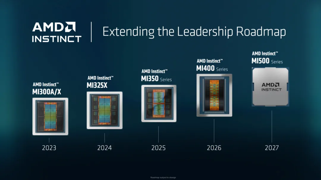
⚙️ MI500 Technical Roadmap (2027) #
The MI500 represents a full generational leap beyond incremental updates.
| Feature | Instinct MI400 (2026) | Instinct MI500 (2027) |
|---|---|---|
| Logic Process | TSMC 3nm | TSMC 2nm |
| Architecture | CDNA 5 | CDNA 6 |
| Memory | HBM4 (~19.6 TB/s) | HBM4E (higher density & bandwidth) |
| Interconnect | Copper (Infinity Fabric) | Optical (CPO) |
| Primary Focus | Peak compute density | Cluster-scale efficiency & latency |
The shift is clear: performance is no longer defined by FLOPS alone.
⚡ Breaking the Copper Limit #
As AI clusters scale to tens of thousands of GPUs, copper interconnects become a bottleneck due to signal loss and power overhead.
What CPO Changes #
-
Shorter Electrical Paths
Optical conversion occurs inside the package, reducing electrical trace length. -
Lower Power Consumption
Estimated 30–40% reduction in interconnect power by minimizing SerDes overhead. -
Higher Bandwidth Density
Optical links scale more efficiently than copper at high speeds. -
Near-Uniform Latency at Scale
Enables clusters of 1,000+ GPUs to behave more like a unified system.
This is essential for training trillion-parameter AI models, where communication dominates compute time.
🆚 AMD vs. NVIDIA: Diverging Strategies #
The competition in optical integration reveals two fundamentally different philosophies.
AMD: Open Ecosystem #
- Partners: TSMC + GlobalFoundries + ASE
- Strength:
- Supply chain diversification
- Potentially better scalability and availability
- Risk:
- Integration complexity across vendors
NVIDIA: Vertical Integration #
- Uses TSMC + Siliconware Precision Industries (SPIL)
- Strength:
- Tight control over design and manufacturing
- Faster iteration cycles
- Risk:
- Dependency on a single ecosystem
AMD is optimizing for resilience and scale, while NVIDIA is optimizing for control and cohesion.
🔬 From Chiplets to Light-on-Chip #
The MI500 signals the next phase of semiconductor evolution:
- From chiplets → optical chiplets
- From compute-bound → interconnect-bound systems
- From electrical scaling → photonic scaling
AMD’s acquisition of Enosemi in 2025 provided the in-house expertise needed to design optical I/O, while GlobalFoundries enables manufacturing at scale.
🧠 Final Insight #
The MI500 shifts the central question in AI hardware:
Not how fast can we compute, but how fast can we move data.
Will AMD’s Strategy Win? #
AMD’s multi-vendor approach could:
- Lower risk of supply bottlenecks
- Improve cost leverage across suppliers
- Enable faster scaling of AI infrastructure
However, it also introduces:
- Integration challenges
- Yield coordination across different process nodes
- Packaging complexity at unprecedented levels
The outcome will likely hinge on execution quality in advanced packaging, not just chip design.