Intel Reports 18A Yield Breakthrough, 30,000 Wafers per Month Capacity, and 14A Roadmap
Intel has reportedly reached an important milestone in its advanced manufacturing strategy. According to recent industry disclosures, the company’s 18A process node has resolved its earlier yield challenges and is now operating at a combined monthly production capacity of approximately 30,000 wafers.
The update also provides new insight into Intel’s next-generation manufacturing roadmap, including the commercialization plans for 18A-P and 14A, two process technologies expected to play a central role in Intel Foundry’s long-term strategy for both internal products and external customers.
Intel’s 18A Yield Challenges Have Reportedly Been Resolved #
According to information cited from BlueFin Research Partners, Intel has overcome the yield issues that affected the early ramp of its 18A manufacturing process.
With these manufacturing challenges addressed, the node is now believed to have reached the operational stability required for sustainable high-volume production, both from a manufacturing efficiency perspective and an economic standpoint.
Intel previously disclosed that yields on the 18A node had been improving at an average rate of roughly 7% per month during the latter stages of development. That steady improvement continued through preparations for Panther Lake, the first commercial processor family manufactured on the 18A process.
The latest industry reports indicate that the major yield-related obstacles have now been eliminated.
Understanding Yield Maturity #
For advanced semiconductor manufacturing, production maturity is typically evaluated using multiple metrics, with defect density (D₀) serving as one of the most closely watched indicators.
Mature production processes generally target a defect density between:
- 0.1 and 0.2 defects per square centimeter
Although Intel has not publicly disclosed official defect-density figures, the reported resolution of yield issues suggests the process may now be operating within a commercially viable range consistent with volume manufacturing.
Achieving this level of manufacturing maturity is a key prerequisite before expanding production to additional products and external foundry customers.
Current Production Capacity Reaches 30,000 Wafers per Month #
Intel’s current 18A manufacturing output is spread across two major facilities:
| Manufacturing Site | Primary Role |
|---|---|
| Fab 52 (Phoenix, Arizona) | High-volume manufacturing |
| D1X (Hillsboro, Oregon) | Process development and production support |
Combined, these facilities are producing approximately:
30,000 wafers per month
According to current estimates, this output is sufficient to support Intel’s near-term internal demand, including production of the upcoming Panther Lake processor family.
As additional internal products transition onto the 18A node, however, Intel will likely need further manufacturing expansion to accommodate increasing wafer demand.
Panther Lake Leads the First Wave of 18A Products #
Panther Lake represents Intel’s first major processor family built on the 18A manufacturing process.
Its launch serves as both a commercial product introduction and a large-scale validation of Intel’s newest process technology.
Successfully supporting Panther Lake production is expected to demonstrate that Intel’s advanced manufacturing roadmap has progressed beyond the development phase into sustained volume manufacturing.
Intel’s Next Step: 18A-P #
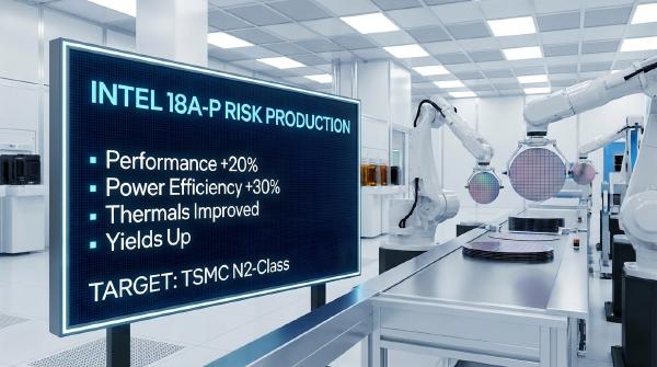
Beyond standard 18A, Intel continues to advance 18A-P, an enhanced derivative process designed to deliver improved performance and power efficiency.
According to current planning:
- Risk production has already begun at the D1X development facility.
- Long-term commercial manufacturing is expected to transition to Fab 62 once production ramps further.
Intel intends 18A-P to become one of the primary offerings for both its internal product portfolio and Intel Foundry customers.
Progress on Intel’s 14A Process #
Intel also provided additional visibility into the company’s next-generation 14A node.
According to current reports:
- Early engineering samples have demonstrated encouraging results.
- Initial development work is progressing as planned.
- Risk production remains scheduled for 2028.
- High-volume manufacturing is targeted for 2029.
The production strategy will follow a phased rollout:
First Production Wave #
- D1X (Hillsboro, Oregon)
Second Production Wave #
- Ohio manufacturing facilities
This staged deployment mirrors Intel’s broader strategy of using D1X as its advanced process development center before transferring mature production to larger manufacturing sites.
Intel Foundry’s Commercial Roadmap #
For external semiconductor customers, Intel Foundry is expected to concentrate on three major process technologies over the coming years:
| Process Node | Planned Status |
|---|---|
| 18A-P | Commercial manufacturing |
| 18A-PT | Commercial offering |
| 14A | Risk production in 2028, mass production in 2029 |
These nodes are expected to form the foundation of Intel’s long-term foundry business as the company competes for customers seeking alternatives to established contract manufacturers.
Manufacturing Roadmap Timeline #
Based on currently available information, Intel’s advanced process roadmap can be summarized as follows:
| Year | Milestone |
|---|---|
| 2026 | 18A reaches stable production and supports Panther Lake |
| 2026–2027 | 18A-P enters risk production and prepares for commercial ramp |
| 2028 | 14A risk production begins |
| 2029 | 14A enters high-volume manufacturing |
This timeline remains broadly aligned with Intel’s publicly announced manufacturing roadmap.
Outlook #
The reported stabilization of Intel’s 18A process represents an important milestone for the company’s manufacturing ambitions. Reaching an estimated production rate of 30,000 wafers per month provides sufficient capacity for current internal products while establishing a foundation for future expansion.
Looking ahead, Intel’s strategy extends beyond 18A. Enhanced variants such as 18A-P and future technologies like 14A are expected to become the cornerstone of both Intel’s own processor roadmap and its growing foundry business.
While industry reports suggest Intel remains on schedule, the long-term competitiveness of these manufacturing nodes will ultimately depend on sustained production yields, continued capacity expansion, customer adoption, and the successful execution of future process transitions.