Huawei’s τ Law: Rethinking Chip Scaling Beyond Moore’s Law
As Moore’s Law approaches both physical and economic limits, the semiconductor industry is being forced to rethink how computing performance can continue scaling in the coming decade. At the IEEE ISCAS conference in Shanghai, Huawei revealed a major shift in its semiconductor research strategy: moving away from traditional geometric scaling and toward what it calls temporal compression.
Internally referred to as Her’s Law, after Huawei executive He Tingbo, the new τ Law framework redefines performance scaling around reducing latency and signal propagation time rather than simply shrinking transistor dimensions.
According to Huawei, this methodology has already been validated across 381 production chips over the past six years, spanning everything from mobile SoCs to large-scale AI computing infrastructure.
🔮 Moving Beyond Traditional Scaling #
For decades, semiconductor advancement has been defined primarily by one question:
Can transistors become smaller?
Moore’s Law enabled the industry to achieve extraordinary gains through geometric miniaturization, allowing transistor density to increase while simultaneously improving power efficiency and performance.
However, modern semiconductor scaling faces growing barriers:
- EUV lithography costs are skyrocketing
- Advanced process nodes are becoming economically restrictive
- Quantum effects increasingly impact transistor behavior
- Interconnect delays now dominate overall latency
- Power density and thermal constraints are intensifying
Huawei’s τ Law reframes the optimization target entirely.
Instead of focusing exclusively on shrinking physical dimensions, the framework asks:
Can the system itself operate faster by compressing time-related bottlenecks?
The underlying insight is that geometric scaling was always indirectly optimizing time. Smaller transistors reduce electrical travel distance, naturally lowering signal propagation delay. Huawei’s engineers concluded that even if physical scaling slows down, engineers can still directly attack the time dimension itself.
⚙️ The Physics Behind τ Scaling #
At the hardware level, signal delay is heavily governed by the RC characteristics of interconnects:
$$ \[ \tau \approx RC \] $$
Where:
- \(R\) represents resistance
- \(C\) represents capacitance
- \(\tau\) represents signal propagation delay
As interconnect length increases, both resistance and capacitance rise, increasing latency along critical execution paths.
Historically, semiconductor scaling reduced these delays by physically shrinking transistors and shortening interconnect distances. Huawei’s approach instead attempts to reduce critical path length through architectural restructuring.
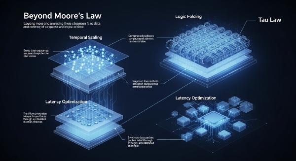
The company calls this methodology Logic Folding.
🏗️ Logic Folding and Vertical Architecture Design #
Traditional chip layouts largely remain constrained to expansive two-dimensional planar designs. Logic Folding introduces a fundamentally different approach by reorganizing critical logic vertically across multiple active layers.
This is enabled through advanced:
- Hybrid bonding
- Multi-layer active silicon stacking
- High-density vertical interconnects
- 3D clock distribution optimization
The concept can be visualized using a simple analogy.
Imagine two distant points on a flat sheet of paper. Traveling between them requires crossing the entire surface. But if the paper is folded so the points align vertically, the effective distance collapses dramatically.
Logic Folding applies this principle directly to semiconductor layouts.
By vertically compressing critical paths, Huawei aims to:
- Reduce parasitic resistance
- Minimize capacitance accumulation
- Lower propagation delay
- Reduce clock skew
- Improve timing closure efficiency
- Increase operational frequency
Rather than relying solely on smaller transistors, performance scaling is achieved through path compression and structural reorganization.
📱 Kirin 2026 Demonstrates the Practical Impact #
Huawei claims the τ Law framework is not merely theoretical. One of the most prominent examples is the company’s Kirin 2026 platform.
Using a two-layer active architecture and what Huawei describes as “Free Logic Design,” the company reportedly achieved substantial gains despite relatively modest transistor density improvements from process technology alone.
Over a three-year period:
- Physical transistor density increased from 1.26 MTr/mm² to 1.55 MTr/mm²
- Effective density reportedly reached 2.38 MTr/mm² through Logic Folding
At the same time, Huawei reports:
- 41% improvement in energy efficiency
- 13% increase in peak frequency
These numbers suggest the company is increasingly prioritizing architectural efficiency over pure lithography progression.
The approach reflects a broader trend across the semiconductor industry: system-level optimization is becoming just as important as transistor-level scaling.
🌐 Scaling Beyond the Chip: “The System Is the Chip” #
Huawei is also applying τ optimization principles at the data center and AI cluster level.
In modern AI infrastructure, data movement has become one of the largest performance bottlenecks. Industry estimates suggest that interconnect and memory movement can account for roughly 80% of total system energy consumption in large AI training clusters.
To address this, Huawei introduced its Unified Bus (UB) architecture.
Rather than relying on traditional protocol-heavy communication layers, UB uses memory-semantic communication techniques designed to reduce conversion overhead and minimize latency.
According to Huawei, this reduces interconnect latency from microseconds to approximately:
$$ \[ 100\text{ ns} \] $$This represents an enormous reduction in communication delay for distributed AI workloads.
The company is also pursuing optical interconnect technologies through its Hi-ONE Optical Interconnect Engine.
Key characteristics include:
- 8 Tb/s bandwidth per module
- Electrical trace lengths reduced to 5 cm
- Rack-to-rack optical reach up to 100 meters
This architecture allows compute resources distributed across multiple racks to behave more like a unified silicon fabric rather than isolated systems.
Huawei summarizes this philosophy with a broader infrastructure principle:
The system itself becomes the chip.
🔬 A Different Path from Industry Giants #
Huawei’s τ Law represents a fundamentally different scaling philosophy compared to other major semiconductor players.
Process Node Leadership #
Companies such as TSMC and Samsung continue focusing heavily on advanced lithography progression:
- 3nm
- 2nm
- Gate-all-around transistors
- EUV process optimization
This remains the traditional continuation of Moore’s Law.
Packaging-Centric Scaling #
Intel has increasingly emphasized advanced packaging technologies alongside node scaling, including:
- Foveros
- EMIB
- Chiplet integration
- 3D stacking
This combines process scaling with heterogeneous integration strategies.
Architecture and Ecosystem Scaling #
NVIDIA’s approach centers on:
- Massive GPU parallelism
- AI-specific architectures
- CUDA ecosystem dominance
- Software-hardware co-optimization
While still dependent on advanced nodes, NVIDIA scales performance heavily through ecosystem leverage and workload specialization.
Huawei’s τ-Centric Strategy #
Huawei’s approach differs at a foundational level.
Rather than depending entirely on access to leading-edge lithography, τ scaling attempts to generate equivalent performance gains through:
- Structural logic reorganization
- Vertical integration
- Critical path compression
- Interconnect optimization
- Hardware-software co-design
- System-level latency reduction
This potentially provides an alternative roadmap when traditional scaling becomes economically or geopolitically constrained.
🌡️ The Major Engineering Challenges Ahead #
Despite its promise, τ scaling introduces substantial engineering complexity.
EDA Toolchain Limitations #
Modern EDA tools were primarily designed around conventional 2D planar layouts.
Free Logic and multi-layer active architectures require:
- New placement algorithms
- 3D-aware routing systems
- Vertical timing analysis
- Thermal-aware optimization
- Novel verification methodologies
Huawei may ultimately need to develop large portions of this design ecosystem independently.
Thermal Density and Power Delivery #
Stacking active layers vertically dramatically intensifies thermal density.
Challenges include:
- Localized thermal hotspots
- Heat extraction complexity
- Power delivery instability
- Transient current spikes
- Cooling path limitations
As chips become denser in three dimensions, thermal engineering evolves from a chip-level optimization problem into a system-scale infrastructure challenge.
🚀 The Long-Term Implications of τ Law #
Huawei projects that future τ-optimized architectures could push effective transistor density beyond:
$$ \[ 400\text{ MTr/mm}^2 \] $$The company also forecasts CPU big-core frequencies surpassing:
$$ \[ 5\text{ GHz} \] $$by 2031 through temporal optimization techniques rather than relying purely on smaller process nodes.
Whether these projections ultimately materialize remains uncertain. However, the broader significance of τ Law is already clear: the semiconductor industry is entering an era where architecture, interconnect design, packaging, and system-level engineering may matter just as much as transistor scaling itself.
Moore’s Law may be slowing, but semiconductor innovation is clearly far from over.