Intel 14A Process Yield Milestone, Roadmap & PDK Update
📊 Yield Progress and Defect Density Status #
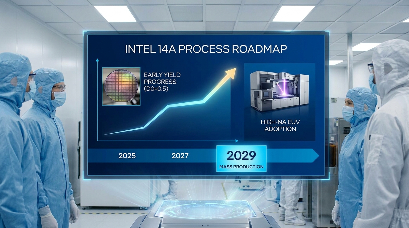
Intel’s 14A process node is currently in an early yield ramp phase, with a reported defect density (D0) of approximately 0.5 according to Morgan Stanley research. At this stage, the node remains pre-mass-production but demonstrates stronger early-stage ramp characteristics compared to Intel’s previous 18A development cycle.
Yield analysis suggests that, under equivalent design conditions, the 14A process already shows improved scaling behavior. For a compute tile comparable in area to Intel’s Panther Lake design, estimated yield reaches ~56.45% under modeled assumptions.
Current test chip data indicates ~40% yield, influenced primarily by larger die area compared to production-target geometries. This aligns with expected early-stage yield constraints in advanced node validation.
⚙️ Yield Modeling and Scaling Behavior #
The reported yield projections are primarily derived from Poisson-based models, where defect density and die area are key variables. As defect density decreases, yield improvements become nonlinear and significantly more sensitive to layout optimization.
When D0 approaches the 0.1–0.2 range, projected yields for ~100 mm²-class dies are estimated to reach 80%–90%, depending on final design complexity and parametric yield constraints.
However, real-world semiconductor yield behavior typically deviates from idealized Poisson assumptions due to systematic defects, layout-dependent failures, and parametric variability across process corners.
Parametric yield remains a critical hidden variable: functional silicon must also meet voltage, frequency, and thermal design targets. These metrics are not yet publicly disclosed for the 14A node.
🗓️ Roadmap: PDK Progress and Production Timeline #
Intel’s 14A development roadmap outlines a staged transition from early validation to high-volume manufacturing:
- Current stage: PDK 0.5 environment
- Target milestone: PDK 0.9 release (expected October, described as a key design-rule stabilization point)
- 2027: Test chip production and early internal product validation
- 2028: Risk production phase with gradual volume scaling
- 2029: Planned mass production ramp
The transition to PDK 0.9 is particularly significant, as it effectively locks design rules and enables customers to finalize tape-out decisions, capacity planning, and product integration strategies.
🔬 High-NA EUV Lithography and Process Stack #
Intel’s 14A node is closely tied to next-generation High-NA EUV lithography adoption in collaboration with ASML. Initial validation includes the TWINSCAN EXE:5000 system, with future integration of the EXE:5200B platform.
These tools are designed to reduce patterning complexity by improving resolution at advanced nodes, enabling tighter feature scaling and potentially reducing multi-patterning steps.
Intel has also reportedly reduced process steps for selected layers from ~40 to under 10 in specific flows, significantly improving manufacturing efficiency and cycle time.
🏭 Manufacturing Efficiency and Wafer Throughput #
Intel has demonstrated quarterly wafer processing volumes exceeding 30,000 wafers, reflecting a mature fabrication throughput baseline.
Workflow optimizations in the 14A development cycle focus on:
- Reduced lithography complexity per layer
- Improved EUV utilization efficiency
- Shorter cycle time per wafer lot
- Higher process repeatability in early ramp phases
These optimizations are essential for improving cost structure and enabling scalable high-volume production once yield stabilization is achieved.
🧭 Implications for Advanced Node Scaling #
The current state of Intel’s 14A process indicates a typical but critical phase in advanced-node development: early defect density reduction combined with lithography and process simplification.
While 18A remains further along in production maturity, 14A serves as a forward-looking node with stronger long-term scaling potential once defect density approaches sub-0.2 levels.
Overall, the roadmap suggests a conventional semiconductor ramp curve: early variability, rapid yield improvement through process tuning, followed by stabilization during risk production and eventual mass manufacturing readiness by the end of the decade.