Intel Reveals Long-Term 14A, 10A, and 7A Process Roadmap
Intel has unveiled new details regarding its long-term semiconductor manufacturing roadmap, signaling that the company intends to remain an aggressive player in the global advanced foundry race well into the next decade.
During the J.P. Morgan Global Technology, Media and Communications Conference, Intel disclosed updated milestones surrounding its upcoming 14A process node while also confirming that research and development work has already begun on even more distant 10A and 7A technologies.
The announcement arrives at a critical moment for the semiconductor industry. Demand for AI computing infrastructure continues to surge globally, placing unprecedented pressure on advanced manufacturing capacity and intensifying competition among leading-edge foundries.
Although Intel spent years facing criticism for repeated manufacturing delays, its newly revealed roadmap suggests a far more ambitious long-term strategy than many industry observers previously assumed.
🏭 Intel’s Manufacturing Reputation Has Been Under Pressure #
Over the past decade, Intel’s process roadmap suffered several highly visible setbacks.
The company experienced:
- Prolonged 10nm delays
- Difficulties transitioning beyond older nodes
- Slower-than-expected EUV adoption
- Intensifying competition from TSMC and Samsung
During this period, many analysts concluded that Intel had permanently lost its process leadership advantage.
Meanwhile, competitors aggressively advanced:
- TSMC’s leading-edge foundry dominance
- AMD’s resurgence through outsourced manufacturing
- Apple’s highly optimized custom silicon strategy
- Nvidia’s explosive AI accelerator growth
This led to growing market narratives portraying Intel as technologically stagnant compared to the broader semiconductor ecosystem.
However, Intel’s latest disclosures indicate that its internal roadmap planning extends far deeper into the future than public perception may suggest.
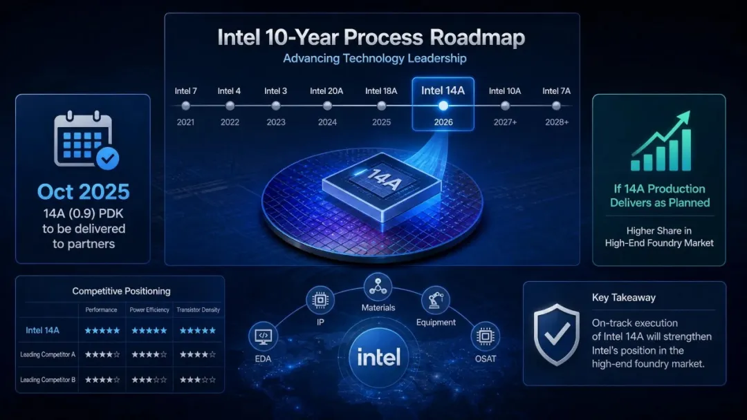
🚀 14A Development Is Reportedly Progressing on Schedule #
At the conference, Intel leadership confirmed that development of the 14A node remains on track.
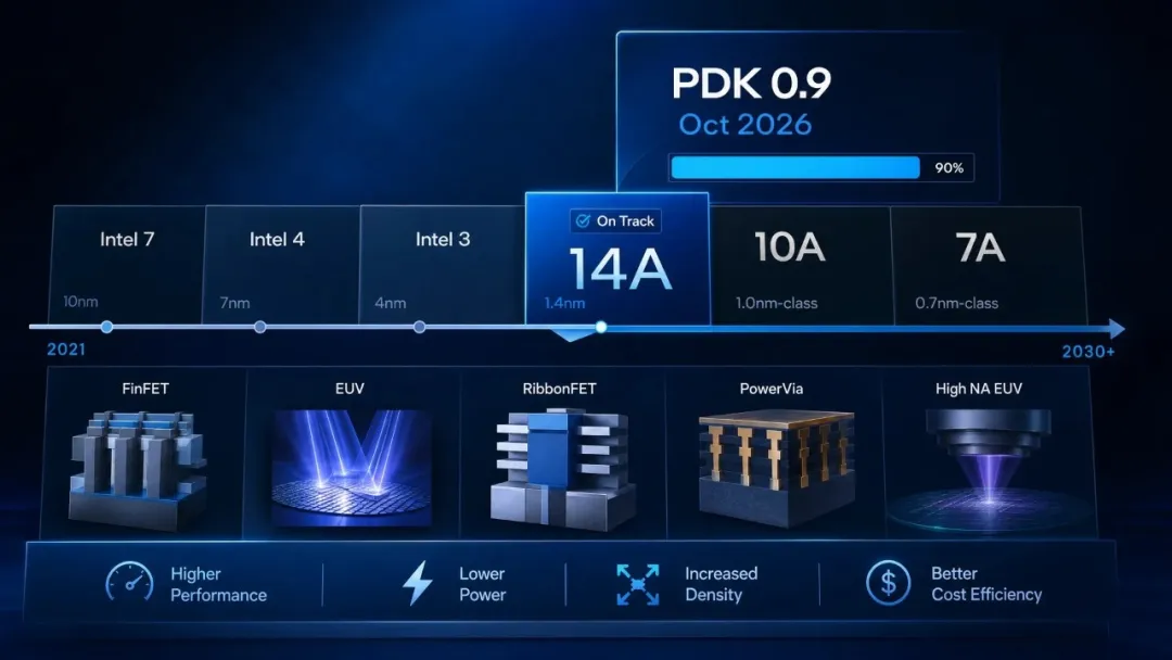
Current milestones include:
- PDK version 0.5 already available
- PDK version 0.9 scheduled for delivery in October
- Early internal customer validation already underway
For semiconductor clients, these milestones matter enormously.
🔧 Why PDK Milestones Matter #
A Process Design Kit (PDK) is effectively the technical foundation that enables chip designers to build products on a foundry’s manufacturing process.
A PDK includes:
- Design rules
- Device models
- Process parameters
- Electrical characteristics
- Verification requirements
- Manufacturing constraints
When a process reaches a mature PDK stage such as version 0.9, it typically signals that:
- Major design rules are stabilizing
- Foundry parameters are nearing production readiness
- Customers can begin more serious product design work
- Large architectural changes become less likely
For major chip designers planning multi-year products, stable PDKs are essential.
⚡ 14A Will Introduce High-NA EUV and PowerVia #
Intel’s 14A node is particularly important because it represents one of the industry’s earliest large-scale deployments of:
- ASML High-NA EUV lithography
- PowerVia backside power delivery
These technologies are viewed as major architectural transitions for advanced semiconductor manufacturing.
🔬 What High-NA EUV Changes #
High-NA (High Numerical Aperture) EUV lithography significantly improves patterning precision compared to traditional EUV systems.
Benefits include:
- Higher transistor density
- Better scaling capability
- Reduced multi-patterning complexity
- Improved feature definition
The technology is widely considered one of the semiconductor industry’s next major manufacturing inflection points.
However, High-NA systems are also:
- Extremely expensive
- Operationally complex
- Difficult to integrate into high-volume production
Only a small number of foundries are expected to deploy them successfully at scale during the late 2020s.
🔋 PowerVia Backside Power Delivery #
Intel’s 14A node also integrates PowerVia backside power delivery.
Traditionally, chips route both:
- Signal interconnects
- Power delivery
through the same front-side metal layers.
PowerVia changes this architecture by moving power routing to the backside of the wafer.
Potential advantages include:
- Lower power delivery resistance
- Reduced congestion
- Better power efficiency
- Higher transistor utilization
- Improved performance scaling
Intel claims this combination of High-NA EUV and PowerVia can deliver approximately:
40% better performance-per-watt
compared to the current 18A node.
🖥️ 14A Is Primarily Targeting High-Performance Computing #
Importantly, Intel appears to be positioning 14A primarily toward:
- AI accelerators
- Data center processors
- HPC infrastructure
- Premium server CPUs
rather than attempting to compete broadly across every semiconductor category simultaneously.
This distinction matters because Intel’s strategy differs somewhat from TSMC’s broader high-volume manufacturing approach.
📅 Intel’s Current 14A Timeline #
According to the disclosed roadmap:
Risk Production #
Expected in 2028
High-Volume Manufacturing #
Targeted for 2029
Intel also confirmed that multiple external customers are already participating in early validation and collaboration efforts, although partner identities remain undisclosed.
🧠 Intel Has Already Started Work on 10A and 7A #
Beyond 14A, Intel also revealed that R&D work has already begun on:
- 10A
- 7A
These future nodes are intended for semiconductor generations extending into the 2030s.
This is notable because advanced process node development cycles now routinely span:
5 to 10 years
before reaching mass production.
🏗️ Why Long-Term Roadmaps Matter So Much #
For modern semiconductor customers, foundry selection increasingly depends on roadmap credibility rather than just current-node performance.
Designing advanced chips now requires enormous lead times.
For example:
High-End Chip Design Timeline #
| Phase | Typical Duration |
|---|---|
| Architecture & Design | 2–3 years |
| Tape-Out & Validation | 1–2 years |
| Mass Production Ramp | Additional months |
As a result, hyperscalers and semiconductor companies need confidence that future process nodes will remain stable and available over long planning horizons.
A delayed process node can disrupt:
- Product launch schedules
- Data center deployment cycles
- AI infrastructure roadmaps
- Entire ecosystem strategies
By publicly disclosing long-range development plans, Intel is effectively signaling:
“Our roadmap is stable enough for customers to plan around.”
That message is critical for rebuilding foundry credibility.
⚔️ Intel and TSMC Are Positioning Differently #
Although comparisons between Intel 14A and TSMC A14 are inevitable, the two companies may not be targeting identical markets initially.
TSMC’s Strategy #
TSMC’s A14 process is expected to prioritize:
- Broad high-volume manufacturing
- Consumer electronics
- Smartphones
- HPC
- Diverse customer portfolios
TSMC traditionally optimizes for:
- Yield stability
- Massive scale
- Ecosystem maturity
Intel’s Strategy #
Intel appears more focused on:
- High-performance computing
- AI infrastructure
- Data center acceleration
- Performance-per-watt optimization
This could allow Intel to avoid direct one-to-one competition in every market segment while focusing resources where margins and strategic importance are highest.
🤖 AI Demand Is Reshaping Foundry Competition #
The explosive growth of AI infrastructure is changing the economics of semiconductor manufacturing.
Global demand for advanced AI accelerators has created:
- Severe leading-edge capacity shortages
- Long procurement lead times
- Supply chain concentration risks
Major customers increasingly want secondary suppliers to reduce dependence on any single foundry ecosystem.
That dynamic potentially creates an opening for Intel Foundry Services.
If Intel successfully executes 14A on schedule, it could become a viable alternative supplier for:
- AI accelerator vendors
- Cloud infrastructure companies
- Enterprise silicon projects
- Government-backed semiconductor initiatives
🌍 Why Diversified Foundry Supply Matters #
The semiconductor industry has become increasingly concentrated around a small number of manufacturing providers.
This concentration introduces several risks:
- Geopolitical instability
- Capacity bottlenecks
- Pricing pressure
- Supply chain fragility
Governments and hyperscalers alike are now actively encouraging supply diversification.
Intel’s long-term roadmap therefore carries significance beyond pure competition.
It potentially contributes to:
- Greater manufacturing redundancy
- Expanded leading-edge capacity
- Reduced systemic supply-chain dependence
📉 Intel Still Faces Major Challenges #
Despite the optimism surrounding the roadmap, Intel’s path forward remains difficult.
The company must still prove it can:
- Deliver nodes on time
- Achieve competitive yields
- Scale High-NA EUV economically
- Attract external customers
- Compete with TSMC’s mature ecosystem
Execution risk remains extremely high in advanced semiconductor manufacturing.
The transition from roadmap presentation to successful high-volume production is where many ambitious plans fail.
🔮 The Foundry Market Is Entering a New Era #
The broader semiconductor industry is entering a phase where:
- Advanced packaging
- Power delivery innovation
- Lithography scaling
- AI-specific optimization
matter just as much as raw transistor density.
Intel’s roadmap suggests the company understands this shift and intends to compete aggressively in AI-oriented manufacturing rather than simply chasing traditional process leadership metrics.
The success of that strategy could significantly reshape the competitive landscape by the end of the decade.
🏁 Conclusion #
Intel’s newly disclosed process roadmap provides a clearer picture of the company’s long-term manufacturing ambitions.
Far from slowing down, Intel appears to be investing heavily into:
- High-NA EUV deployment
- Backside power delivery
- AI-focused process optimization
- Multi-generation foundry planning
The 14A node represents a critical milestone not only for Intel itself, but also for the broader balance of power within the global semiconductor industry.
If Intel can execute its roadmap successfully, the advanced foundry market may evolve from today’s highly concentrated structure into a more competitive and diversified ecosystem.
For hyperscalers, AI companies, and global semiconductor customers, that possibility alone makes Intel’s roadmap worth watching closely over the next several years.