
Intel EMIB-T Challenges CoWoS with Up to 50% Lower Packaging Costs
Intel has disclosed new details about EMIB-T, the next evolution of its Embedded Multi-die Interconnect Bridge (EMIB) packaging technology. Positioned as a high-performance alternative to TSMC’s CoWoS, EMIB-T is designed for chiplet-based processors, AI accelerators, and custom ASICs, with Intel targeting high-volume production in 2027.
According to recently disclosed information, EMIB-T could reduce advanced packaging costs by up to 50% compared with certain CoWoS implementations while supporting multi-kilowatt package designs and high-bandwidth memory (HBM) integration. If these claims are realized in commercial products, EMIB-T could become a compelling option for customers seeking to balance performance, scalability, and manufacturing costs.
Several major AI chip developers, including Broadcom and Meta, are reportedly evaluating Intel’s packaging technology as an alternative to existing CoWoS-based solutions.
📦 EMIB-T Extends Intel’s Advanced Packaging Portfolio #
Intel introduced EMIB (Embedded Multi-die Interconnect Bridge) to enable high-density interconnects between multiple dies without relying on a full silicon interposer.
Unlike traditional 2.5D packaging approaches, EMIB embeds small silicon bridges directly into the package substrate, providing localized die-to-die communication while reducing manufacturing complexity.
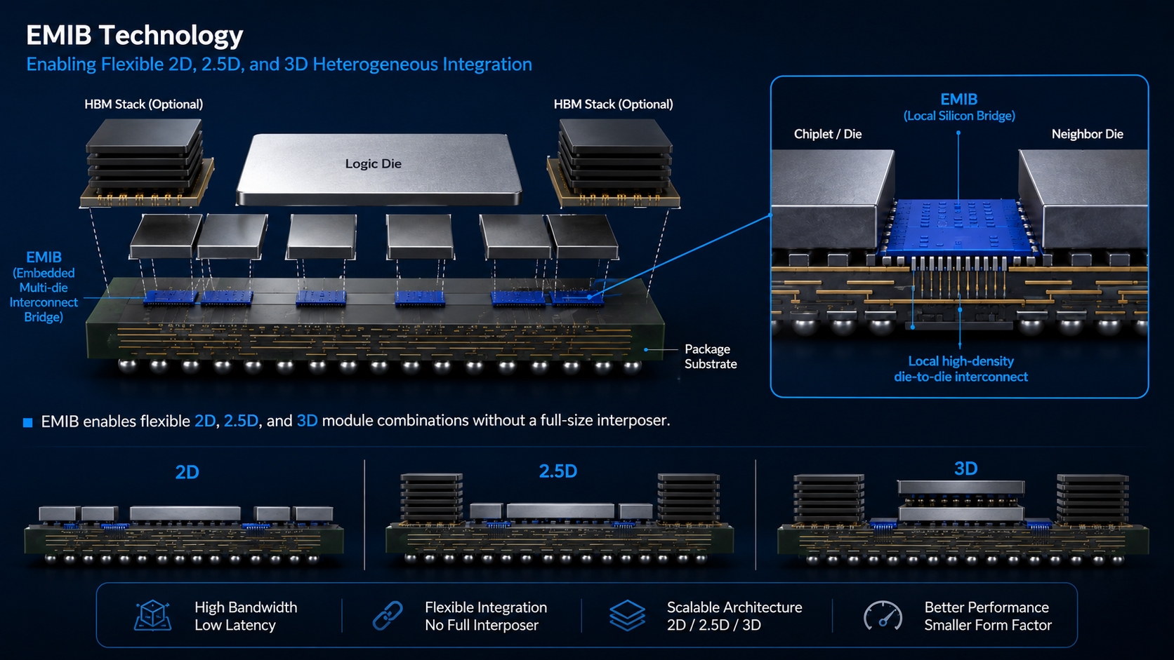
The technology supports a variety of packaging configurations, including:
- 2D integration
- 2.5D integration
- 3D stacking
This flexibility allows chip designers to select the packaging architecture best suited to their performance, power, and cost requirements.
How EMIB Differs from Full Interposer Designs #
Many advanced packaging solutions use a large silicon interposer beneath all chiplets to provide high-density interconnections.
While effective, full interposers significantly increase manufacturing costs due to their size and complexity.
EMIB instead places silicon bridges only where high-bandwidth communication is required.
This localized approach offers several potential advantages:
- Lower packaging costs
- Reduced silicon area
- High-bandwidth die-to-die communication
- Greater packaging flexibility
For heterogeneous chiplet architectures, these characteristics can improve overall manufacturing efficiency without sacrificing interconnect performance.
⚡ EMIB-T Adds Through-Silicon Via Technology #
EMIB-T expands the original EMIB architecture by incorporating Through-Silicon Vias (TSVs).
The addition of TSVs enables more efficient power delivery within complex multi-die packages.
According to Intel, EMIB-T allows ASICs to access dedicated power connections directly through the package structure, supporting:
- Logic-to-logic interconnects
- Logic-to-HBM integration
- Multi-kilowatt package power delivery
As AI accelerators continue increasing in power consumption, efficient power distribution becomes just as important as high-bandwidth communication between compute dies and memory.
Direct power delivery through TSV-enabled packaging is therefore expected to play a growing role in next-generation AI hardware.
🏭 High-Volume Production Planned for 2027 #
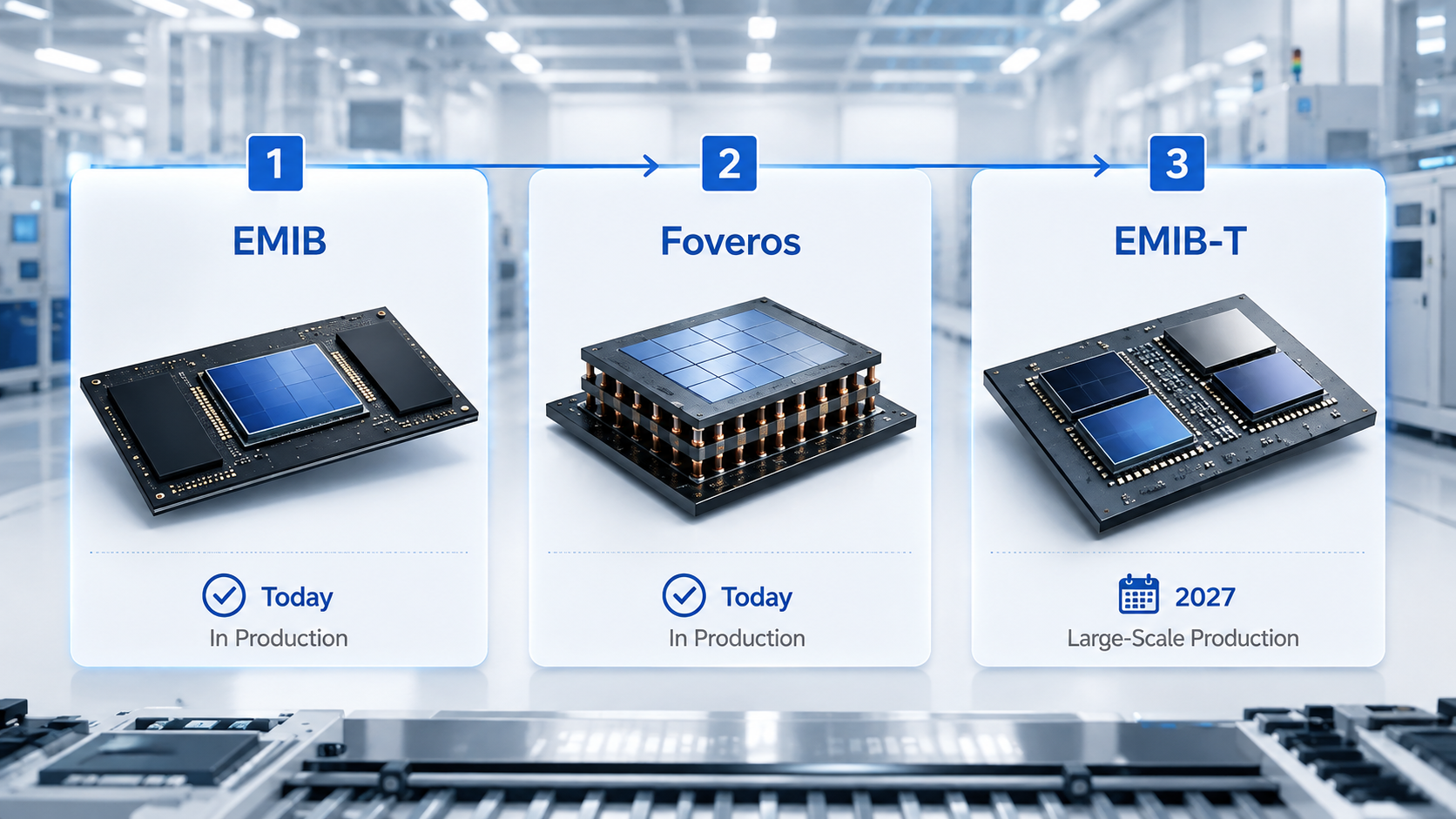
Intel indicated that its standard EMIB and Foveros packaging technologies are already progressing through customer production ramps.
EMIB-T represents the next stage of that roadmap, with high-volume manufacturing targeted for 2027.
Until then, customers requiring advanced packaging can continue deploying products based on Intel’s existing EMIB platform while preparing future designs for EMIB-T.
The reported production timeline was disclosed through information shared by PCB and substrate manufacturer Unimicron, highlighting growing industry attention toward Intel Foundry’s advanced packaging capabilities.
As packaging increasingly becomes a strategic differentiator in semiconductor manufacturing, technology roadmaps such as EMIB-T may influence future foundry selection alongside wafer fabrication capabilities.
💰 Up to 50% Lower Packaging Costs #
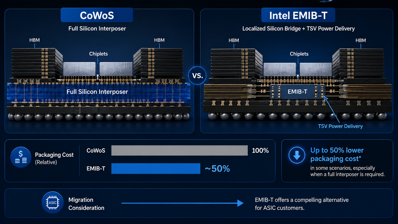
One of EMIB-T’s most significant selling points is its projected cost advantage.
Intel positions the technology as a direct competitor to TSMC CoWoS, claiming that certain packaging configurations can reduce costs by as much as 50%.
The exact savings depend largely on package architecture.
Designs that would otherwise require expensive full-size silicon interposers are expected to benefit the most from EMIB-T’s bridge-based approach.
For large AI processors containing multiple compute chiplets and stacks of HBM memory, packaging costs represent a substantial portion of overall manufacturing expenses.
Reducing those costs can improve product economics without requiring changes to chip architecture.
🤖 AI Chip Designers Are Evaluating the Technology #
Reports indicate that several major custom silicon developers are exploring Intel’s packaging solutions.
Among the companies reportedly evaluating a transition are:
- Broadcom
- Meta
Both organizations develop large-scale AI accelerators and custom ASICs that depend heavily on advanced packaging technologies.
If these companies adopt EMIB-T in future products, it could demonstrate Intel’s ability to compete not only in wafer manufacturing but also in advanced heterogeneous integration.
Successful deployments from major hyperscale customers would likely encourage broader industry adoption across other AI and high-performance computing projects.
📈 Why Advanced Packaging Matters More Than Ever #
As semiconductor scaling becomes increasingly complex, advanced packaging has evolved into a critical competitive technology rather than a secondary manufacturing step.
Modern AI accelerators frequently combine:
- Multiple compute chiplets
- High-bandwidth memory (HBM)
- Specialized I/O dies
- High-speed interconnect fabrics
Packaging determines how efficiently these components communicate, how much power can be delivered, and how economically the final product can be manufactured.
For AI infrastructure providers deploying hundreds of thousands of accelerators, even modest reductions in packaging costs can translate into significant savings across an entire deployment.
Those savings may be reinvested into:
- Larger wafer allocations
- Additional HBM capacity
- More advanced chip designs
- Expanded production volumes
🔮 Outlook #
Intel has yet to release comprehensive technical benchmarks or commercial performance data for EMIB-T, and many implementation details—including initial production customers and real-world cost reductions—remain undisclosed.
Nevertheless, the technology represents an important step in Intel Foundry’s broader strategy to compete beyond traditional semiconductor fabrication. By combining advanced packaging technologies such as EMIB, Foveros, and the upcoming EMIB-T, Intel is positioning itself to address one of the fastest-growing segments of the semiconductor industry: heterogeneous integration for AI and high-performance computing.
As chiplet-based architectures continue to replace monolithic processor designs, advanced packaging will become increasingly central to product competitiveness. If EMIB-T delivers the projected cost advantages while maintaining the performance required by next-generation AI accelerators, it could emerge as one of the most significant alternatives to CoWoS in the years ahead.