Intel Nova Lake: Massive Die Size Increase for a Gaming Breakthrough?
As Intel’s Core Ultra 400 series (Nova Lake-S) targets a late-2026 launch window, attention has shifted to one striking architectural shift: a dramatic increase in compute tile area.
After Arrow Lake’s mixed gaming reception—particularly around latency sensitivity and cache hierarchy—Intel appears to be responding with brute-force silicon scale.
The strategy centers around one concept: bLLC.
🔮 bLLC: Big Last-Level Cache Integration #
The most significant Nova Lake rumor is the integration of bLLC (big Last Level Cache) directly inside the compute tile.
Unlike AMD’s vertically stacked 3D V-Cache approach, Intel’s solution expands the cache laterally on the same silicon plane as the CPU cores.
Reported Die Area Changes #
- Standard Compute Tile: ~110 mm²
- Nova Lake Compute Tile: ~150 mm²
- Increase: +40 mm² (~36%)
That additional 40 mm² is reportedly dominated by expanded L3 SRAM arrays.
Since SRAM is area-expensive, this strongly implies:
- A major L3 capacity increase
- Reduced memory access latency
- Improved frame time consistency in cache-sensitive gaming workloads
Intel is effectively trading die efficiency for lower latency and higher sustained gaming performance.
🎮 Why Cache Size Matters for Gaming #
Modern game engines are increasingly sensitive to:
- Asset streaming latency
- Large world-state data structures
- AI pathfinding buffers
- Physics simulation memory locality
A larger L3 cache:
- Reduces round trips to DRAM
- Improves minimum frame rates (1% lows)
- Stabilizes CPU-limited scenarios
Arrow Lake’s weakness wasn’t raw compute—it was memory hierarchy efficiency under gaming loads. Nova Lake’s enlarged cache directly targets that bottleneck.
⚙️ The Manufacturing Trade-Off #
A 150 mm² compute tile is not a trivial escalation.
Yield Risk #
Larger dies statistically suffer:
- Higher defect probability
- Lower per-wafer usable output
- Increased binning complexity
If this size becomes mainstream rather than halo-tier, manufacturing economics tighten significantly.
Advanced Packaging Complexity #
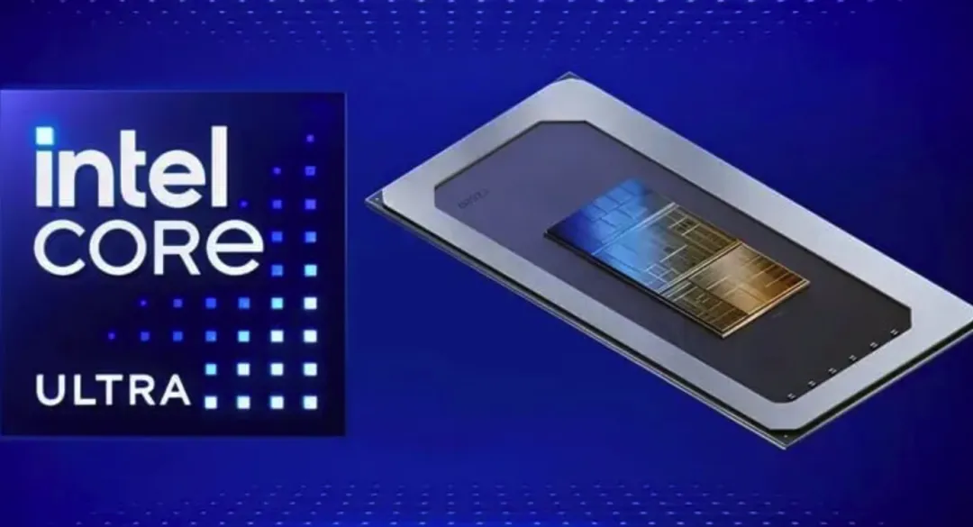
Nova Lake continues Intel’s tiled strategy under Foveros Advanced packaging, combining:
- Compute tile (with bLLC)
- SoC tile
- I/O tile
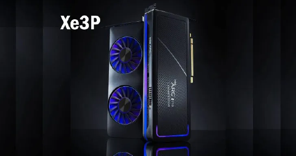
- Xe3P GPU tile
While disaggregation improves modularity, it increases:
- Interconnect validation complexity
- Power delivery engineering difficulty
- Thermal balancing challenges
Cost & Pricing Implications #
More silicon area per chip means:
- Higher wafer cost per unit
- Tighter margin sensitivity
- Potential DIY market price increases
Unless Intel achieves strong yields on Intel 18A and/or TSMC N2 nodes, Nova Lake could launch at a noticeable premium.
🏗️ Cache Hierarchy Evolution #
Nova Lake reportedly rebalances both L2 and L3 structures.
| Feature | Arrow Lake | Nova Lake (Core Ultra 400) |
|---|---|---|
| L2 Cache | 3MB per P-core | 4MB per P-core pair (shared) |
| L3 Cache | Standard configuration | Massive bLLC integration |
| GPU Tile | Xe-LPG | Xe3P (Nova Graphics) |
| Process Node | Intel 20A / TSMC N3 | Intel 18A / TSMC N2 |
The L2 adjustment suggests Intel is optimizing for:
- Better core-to-core data sharing
- Reduced duplication overhead
- Balanced latency tiers
Combined with a larger L3 pool, Nova Lake may significantly reshape Intel’s gaming memory hierarchy behavior.
⚖️ Intel vs AMD: Silicon Budget Strategy #
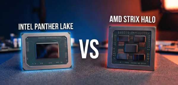
Rumors indicate AMD’s upcoming Zen 6 compute tile (TSMC N2 nanosheet process) may occupy roughly 76 mm², potentially delivering similar core counts in half the area.
Strategic Contrast #
Intel Approach
- Increase silicon footprint
- Expand cache laterally
- Prioritize gaming latency gains
AMD Approach
- Leverage advanced process density
- Maintain smaller compute tile
- Optimize performance-per-watt
Intel is effectively spending “silicon budget” to close the gaming gap, while AMD may rely on node efficiency and architectural scaling.
This is a philosophical divergence:
- Horizontal cache expansion vs density-driven scaling
- Area-heavy latency mitigation vs transistor efficiency
🔥 Thermal & Structural Implications #
By integrating cache on-die rather than stacking vertically:
Advantages #
- Avoids 3D stacking thermal resistance
- Simplifies heat dissipation pathways
- Maintains traditional cooling compatibility
Disadvantages #
- Consumes significant planar area
- Reduces die-per-wafer count
- Raises cost sensitivity
Nova Lake resembles a semi-monolithic philosophy executed within a tiled framework.
🎯 The High-Stakes Question #
Intel’s gamble is straightforward:
Does +40 mm² of additional L3 cache finally neutralize AMD’s gaming leadership?
If cache expansion meaningfully improves:
- 1% low frame rates
- CPU-bound 1080p gaming benchmarks
- Latency-sensitive esports titles
Then Nova Lake may mark Intel’s true gaming comeback.
If not, the increased die size becomes an expensive experiment.
🧩 Final Perspective #
Nova Lake is not incremental—it is strategic escalation.
By materially enlarging its compute tile, Intel signals:
- Aggressive competitive intent
- Willingness to trade area for latency
- Confidence in advanced packaging and 18A process maturity
The 2026 desktop battle may ultimately hinge not on core counts—but on cache topology.
And this time, Intel is betting big—literally.