Intel Becomes First to Mass Produce High-NA EUV Logic Chips
The semiconductor industry’s next major manufacturing breakthrough has officially moved from research labs into commercial production. On July 15, 2026, ASML confirmed that Intel Foundry has become the first semiconductor manufacturer to mass-produce and ship commercial logic chips fabricated using High-NA (0.55 Numerical Aperture) EUV lithography.
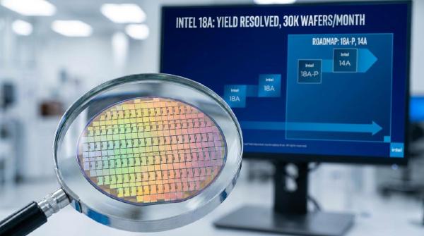
The technology is currently deployed on selected layers of Intel’s 18A process node, where it is being used to manufacture portions of the company’s Core Ultra Series 3 “Panther Lake” processors. The achievement marks the first commercial validation of High-NA EUV in a high-volume manufacturing environment and establishes Intel as the industry’s earliest adopter of the technology.
🔬 Understanding High-NA EUV Lithography #
Lithography is the core process used to transfer circuit patterns onto silicon wafers. Modern leading-edge manufacturing relies on Extreme Ultraviolet (EUV) light with a wavelength of 13.5 nanometers to pattern increasingly dense transistor structures.
While both conventional EUV and High-NA EUV utilize the same wavelength, the key distinction lies in the optical system’s Numerical Aperture (NA), which determines how effectively the scanner can collect and focus light onto the wafer.
| Lithography Platform | Numerical Aperture |
|---|---|
| Standard EUV (ASML NXE Series) | 0.33 NA |
| High-NA EUV (ASML EXE Series) | 0.55 NA |
The increase from 0.33 NA to 0.55 NA significantly improves imaging resolution, allowing chipmakers to print smaller and denser features with greater precision.
Why Higher Numerical Aperture Matters #
As transistor dimensions continue to shrink, conventional EUV increasingly relies on complex multi-patterning techniques to print dense layouts.
Multi-patterning requires the same circuit layer to be divided across multiple exposures, increasing:
- Process complexity
- Cycle time
- Overlay requirements
- Defect opportunities
- Manufacturing costs
High-NA EUV reduces this burden by enabling more aggressive feature scaling through single-exposure patterning on selected layers. The result is improved process efficiency and a clearer path toward future Angstrom-class nodes.
🏭 Intel’s Manufacturing Achievement #
Introducing an entirely new lithography platform into production is only valuable if manufacturing yields remain competitive.
What distinguishes Intel’s deployment is not simply the use of High-NA EUV, but the successful integration of the technology into a commercial production flow while maintaining operational flexibility.
Yield Parity with Conventional EUV #
Intel and ASML confirmed that Panther Lake products utilizing High-NA EUV are achieving yields comparable to equivalent layers produced using traditional 0.33 NA EUV systems.
Achieving yield parity at this stage is a significant milestone because advanced lithography transitions have historically introduced prolonged yield-learning cycles before reaching production maturity.
Dual-Qualified Process Layers #
One of the most important aspects of Intel’s strategy is the implementation of dual-qualified process layers.
Selected 18A layers can be manufactured using either:
- ASML’s High-NA EXE scanners
- Conventional NXE EUV scanners
This dual-path approach provides substantial operational flexibility during the early stages of High-NA deployment.
Supply Chain Resilience #
Because the same layers can be processed on both toolsets, Intel can redirect production if a High-NA system undergoes maintenance, calibration, or process optimization.
Rather than creating a bottleneck around a small number of new scanners, Intel preserves manufacturing continuity while continuing to refine High-NA production processes.
⚔️ Intel and TSMC Take Different High-NA Paths #
For much of the past decade, TSMC has been widely viewed as the leader in advanced semiconductor manufacturing. However, the industry’s first commercial High-NA deployment has shifted the narrative—at least temporarily—in Intel’s favor.
| Foundry | High-NA EUV Status | Strategy |
|---|---|---|
| Intel Foundry | Commercial production in 2026 | Early adoption through 18A, building production experience ahead of 14A |
| TSMC | Estimated adoption around 2029–2030 | Extending conventional EUV and multi-patterning before transitioning to High-NA |
Intel acquired the world’s first commercial ASML TWINSCAN EXE:5000 system in 2024 and later expanded its deployment with the higher-throughput EXE:5200B platform.
Rather than waiting for the technology to mature further, Intel chose to absorb the learning curve early, using 18A as a proving ground before broader deployment on future nodes.
TSMC, by contrast, has pursued a more conservative strategy. The company has indicated that conventional EUV remains economically viable for upcoming process generations and has chosen to continue optimizing multi-patterning techniques rather than immediately adopting High-NA EUV.
The decision is understandable given the economics involved. High-NA scanners are estimated to cost approximately $400 million per system, making them among the most expensive manufacturing tools ever deployed in semiconductor production.
🚀 From Panther Lake to the Angstrom Era #
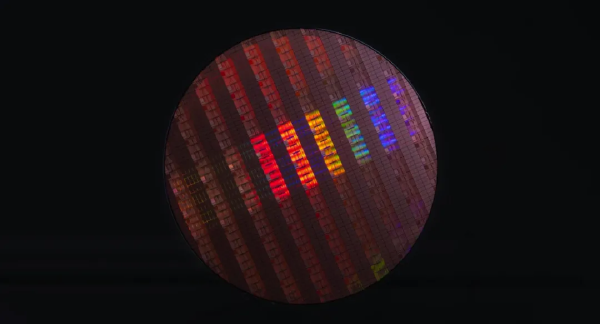
The High-NA-enabled wafers currently being shipped originate from Intel’s manufacturing facilities in Hillsboro, Oregon, and are progressing through packaging and assembly operations as part of Intel’s broader product rollout.
The Panther Lake launch timeline has already progressed through multiple commercial milestones:
| Date | Milestone |
|---|---|
| January 5, 2026 | Core Ultra Series 3 (Panther Lake) introduced at CES |
| January 27, 2026 | Global retail availability begins |
| Spring 2026 | Wildcat Lake processors and Arc G3 handheld products enter the market |
The successful deployment of High-NA EUV on 18A provides Intel with valuable real-world manufacturing experience, including process integration, photoresist behavior, defect management, overlay control, and production-scale tool operation.
These lessons are expected to play a critical role in the development of Intel’s next-generation 14A process node.
⚙️ High-NA EUV and Intel 14A #
Intel views 18A as the first step in a broader High-NA roadmap rather than the technology’s final destination.
According to Intel Foundry leadership, qualifying High-NA process options on selected 18A layers creates additional manufacturing flexibility while laying the groundwork for more extensive adoption on future nodes.
As minimum feature pitches continue to shrink, Intel 14A is expected to utilize High-NA EUV across a broader range of critical layers, allowing the company to further improve transistor density, manufacturing efficiency, and process scalability.
In practical terms, 18A serves as the industry’s first commercial validation of High-NA EUV, while 14A is expected to be the node where the technology becomes a foundational manufacturing capability.
📈 Industry Significance #
Intel’s successful commercial deployment represents a major milestone not only for the company but for the semiconductor industry as a whole.
High-NA EUV has long been viewed as one of the most important technologies required to sustain Moore’s Law beyond conventional EUV limits. By moving the technology into volume production, Intel and ASML have demonstrated that High-NA lithography is no longer a future concept—it is now an operational manufacturing technology.
Whether Intel’s early investment ultimately translates into a sustained competitive advantage remains to be seen. However, the company now possesses years of real-world High-NA experience that competitors have yet to accumulate.
As semiconductor manufacturing enters the Angstrom era, that experience could prove just as valuable as the technology itself.