Intel Spins Off Advanced Packaging Unit Under Seok-Hee Lee
📘 Executive Summary #
Intel has announced a major organizational restructuring alongside a high-profile executive appointment aimed at strengthening its foundry business and accelerating its position in the rapidly growing advanced packaging market.
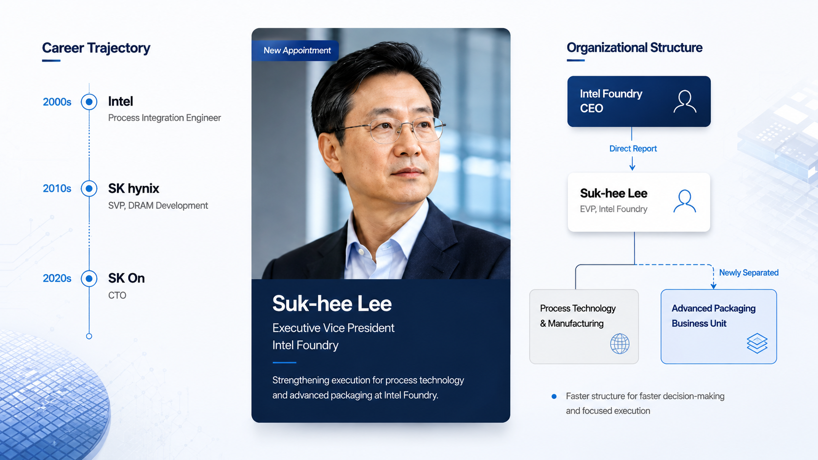
Former SK Hynix and SK On CEO Seok-Hee Lee has been appointed Executive Vice President of Intel Foundry and will lead a newly independent business unit focused on advanced packaging, system integration, back-end technology development, and high-volume manufacturing operations.
The move reflects Intel’s increasing emphasis on packaging technologies as a strategic differentiator in the AI era. As traditional transistor scaling becomes more challenging and expensive, advanced packaging has emerged as a critical enabler for next-generation computing platforms, allowing manufacturers to combine multiple chiplets, memory stacks, and accelerators into highly integrated systems.
By establishing a dedicated packaging organization with direct executive oversight, Intel aims to improve operational execution, attract high-value AI customers, and strengthen the financial performance of its foundry division.
⚙️ Leadership and Strategic Metadata #
| Attribute | Details |
|---|---|
| Executive Appointment | Seok-Hee Lee, Executive Vice President, Intel Foundry |
| Reporting Structure | Directly reports to Lip-Bu Tan |
| Business Scope | Advanced Packaging, System Integration, Back-End Manufacturing |
| Strategic Focus | AI Infrastructure and Heterogeneous Computing |
| Primary Competitive Target | TSMC Advanced Packaging Ecosystem |
| Potential Customer Engagements | Large Hyperscale and Cloud Providers |
| Announcement Period | June 2026 |
🏗️ Why Advanced Packaging Has Become a Strategic Priority #
The semiconductor industry is undergoing a fundamental architectural transition.
For decades, performance improvements were primarily achieved through transistor scaling. However, as process technologies approach economic and physical limits, chip manufacturers increasingly rely on advanced packaging to deliver higher performance, improved power efficiency, and greater system-level integration.
Modern AI accelerators, high-performance computing processors, and cloud infrastructure platforms often combine:
- Multiple compute chiplets
- High-bandwidth memory (HBM)
- Specialized AI accelerators
- Networking components
- I/O dies
These components must communicate with extremely high bandwidth and low latency, making packaging technology a key competitive advantage.
As a result, advanced packaging has evolved from a manufacturing support function into a core technology platform that directly influences system performance, power efficiency, scalability, and profitability.
👤 Seok-Hee Lee’s Appointment and Industry Experience #
Intel’s selection of Seok-Hee Lee highlights the company’s focus on manufacturing discipline and operational execution.
Lee brings a unique combination of experience from both Intel and the South Korean semiconductor industry.
His background includes:
- Early engineering leadership experience at Intel
- Executive management roles in semiconductor manufacturing
- Leadership of SK Hynix, one of the world’s largest memory manufacturers
- Experience overseeing high-volume production environments
- Expertise in yield optimization and manufacturing scale-up
This blend of technical and operational knowledge is particularly relevant for advanced packaging, where manufacturing complexity continues to increase alongside AI-driven demand.
🔄 Foundry Organization Restructuring #
The creation of a standalone packaging business unit is part of a broader restructuring effort within Intel Foundry.
Direct Executive Alignment #
Under the new structure, Seok-Hee Lee will report directly to Intel Foundry leadership, reflecting the strategic importance of packaging technologies within the company’s long-term roadmap.
This reporting model is designed to:
- Accelerate decision-making
- Improve execution speed
- Increase accountability
- Streamline customer engagement
Front-End and Back-End Separation #
The restructuring creates clearer organizational boundaries between manufacturing disciplines.
Front-end semiconductor development remains focused on:
- Process technology innovation
- Wafer fabrication
- Leading-edge node deployment
- Technology scaling
Meanwhile, the new packaging organization assumes responsibility for:
- Advanced packaging platforms
- Heterogeneous integration
- System assembly
- Back-end manufacturing optimization
This specialization enables each group to concentrate on its respective technology challenges.
Leadership Transition #
The restructuring also coincides with broader leadership changes within Intel’s manufacturing organization, including executive realignments and veteran retirements that reflect the company’s ongoing transformation efforts.
🚀 Intel’s Advanced Packaging Technology Roadmap #
A central responsibility of the new business unit will be scaling Intel’s next-generation packaging technologies for commercial deployment.
🔗 EMIB-T: Next-Generation Multi-Die Integration #
One of the flagship technologies under development is EMIB-T, an evolution of Intel’s Embedded Multi-die Interconnect Bridge architecture.
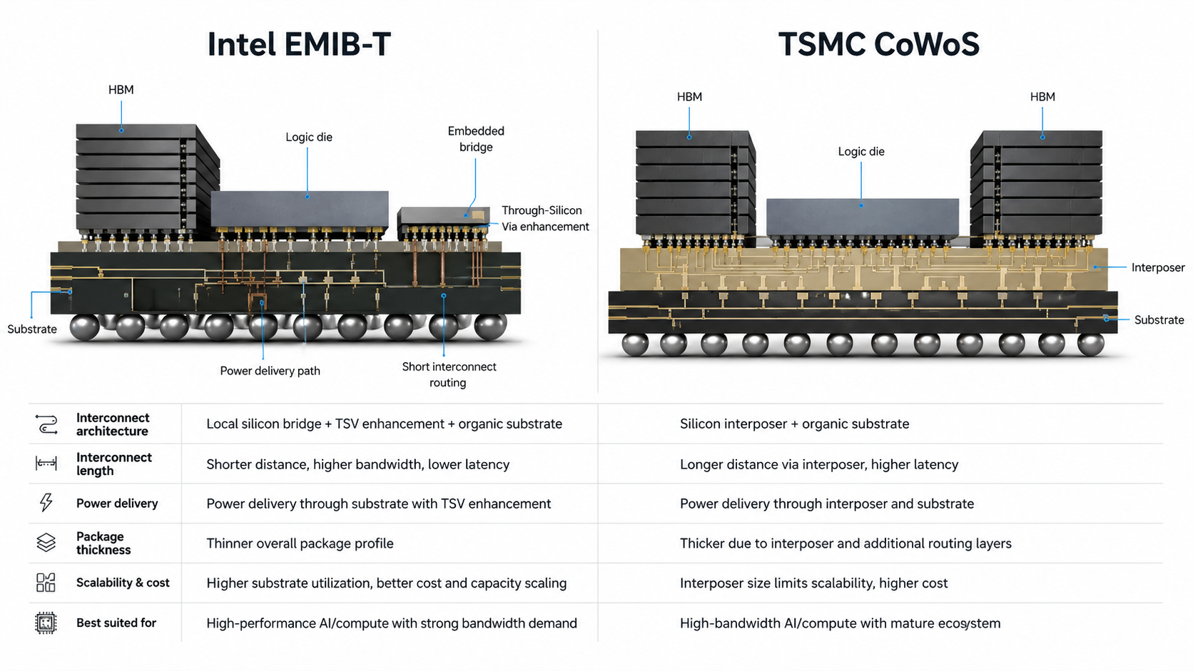
What EMIB-T Enables #
EMIB technology provides high-density interconnect pathways between multiple silicon dies without requiring a full silicon interposer.
The enhanced EMIB-T architecture introduces:
- Through-Silicon Via (TSV) integration
- Increased routing density
- Improved signal integrity
- Enhanced power delivery capabilities
- Greater scalability for AI workloads
Supporting Future HBM4 Architectures #
The technology is specifically designed to address the demands of future High-Bandwidth Memory (HBM4) deployments.
Modern AI accelerators require massive memory bandwidth to feed increasingly large compute arrays. As memory bandwidth requirements continue to rise, packaging solutions become critical bottlenecks.
EMIB-T aims to provide:
- Higher interconnect density
- Lower latency communication
- Improved energy efficiency
- Better support for multi-chip AI systems
🧠 HBI: Hybrid Bonding Interconnect #
Another key technology under development is Hybrid Bonding Interconnect (HBI).
Moving Beyond Traditional Packaging #
Unlike conventional package-level interconnects, hybrid bonding enables direct copper-to-copper connections between stacked dies.
This approach delivers several advantages:
- Extremely fine interconnect pitch
- Reduced signal loss
- Lower parasitic capacitance
- Improved power efficiency
- Higher communication bandwidth
Enabling 3D System Architectures #
Hybrid bonding is increasingly viewed as a foundational technology for future 3D semiconductor architectures.
Potential applications include:
- AI accelerators
- High-performance computing processors
- Memory-on-logic integration
- Chiplet-based architectures
- Advanced heterogeneous systems
As the industry moves toward vertically integrated designs, technologies like HBI become increasingly important for achieving performance gains beyond traditional scaling methods.
🤖 AI Infrastructure as the Primary Growth Driver #
The rapid expansion of artificial intelligence infrastructure has transformed advanced packaging into one of the fastest-growing segments of semiconductor manufacturing.
Modern AI systems depend heavily on:
- Massive compute density
- High-bandwidth memory integration
- Multi-chip packaging architectures
- Advanced interconnect technologies
Consequently, cloud providers and hyperscale operators are investing heavily in packaging-intensive accelerator platforms.
Intel’s packaging expansion is therefore closely aligned with broader AI infrastructure demand.
💰 Financial Motivation Behind the Restructuring #
The creation of a standalone packaging organization is driven not only by technology strategy but also by financial objectives.
Higher-Margin Business Opportunity #
Advanced packaging services generally offer:
- Higher value-add differentiation
- Stronger customer lock-in
- Greater technical barriers to entry
- Premium pricing opportunities
As demand for AI accelerators grows, packaging has become one of the most attractive profit pools within the semiconductor value chain.
Supporting Foundry Profitability #
Intel continues to pursue long-term profitability improvements across its foundry business.
The packaging segment is viewed as a potential contributor due to:
- Strong industry demand
- Growing customer interest
- Expanding AI workloads
- Increased adoption of chiplet architectures
A successful packaging business could help improve overall foundry economics while strengthening Intel’s competitive position.
🌎 Competitive Implications #
Advanced packaging has become one of the most fiercely contested areas in semiconductor manufacturing.
Industry leaders increasingly compete not only on process nodes but also on system integration capabilities.
Key competitive battlegrounds include:
- Chiplet integration
- HBM packaging
- 2.5D architectures
- 3D stacking technologies
- High-volume manufacturing execution
Intel’s decision to elevate packaging into an independent business unit demonstrates how strategically important these technologies have become.
Success will depend on the company’s ability to:
- Deliver competitive packaging platforms
- Scale production efficiently
- Maintain high yields
- Attract major AI customers
- Execute complex manufacturing programs reliably
📈 Industry Outlook #
The semiconductor industry is entering an era where packaging innovation may contribute as much to system performance as process-node advancements.
Several trends are expected to accelerate demand:
- Growth of generative AI infrastructure
- Expansion of chiplet-based architectures
- Adoption of HBM4 memory systems
- Increasing complexity of heterogeneous computing platforms
- Demand for higher performance-per-watt
Companies capable of delivering advanced packaging solutions at scale are likely to gain significant competitive advantages in both the foundry and AI hardware markets.
🏁 Conclusion #
Intel’s appointment of Seok-Hee Lee and the creation of an independent advanced packaging business unit represent a significant strategic shift within its foundry organization. By separating packaging and system integration into a dedicated operational track, Intel is positioning itself to compete more aggressively in one of the semiconductor industry’s fastest-growing and highest-value segments.
With technologies such as EMIB-T and Hybrid Bonding Interconnect at the center of its roadmap, the company is betting that advanced packaging will play a defining role in the future of AI computing, heterogeneous integration, and next-generation semiconductor design.
Whether the strategy ultimately translates into stronger foundry profitability and broader market share gains will depend on execution, customer adoption, and Intel’s ability to scale advanced packaging technologies into high-volume manufacturing. However, the restructuring clearly signals that packaging is no longer viewed as a supporting function—it is now a core pillar of Intel’s semiconductor strategy.