JEDEC SPHBM4 Standard Cuts HBM Packaging Costs Without CoWoS
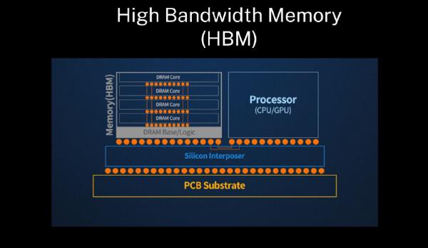
High Bandwidth Memory (HBM) has become a cornerstone of modern AI accelerators, but its widespread adoption has been constrained by one major challenge: advanced packaging. Traditional HBM implementations depend on silicon interposers and technologies such as CoWoS, making manufacturing expensive and limiting production capacity.
To address this bottleneck, JEDEC has officially published the JESD330-4 SPHBM4 specification. Rather than replacing HBM4, SPHBM4 introduces a more cost-effective implementation that preserves HBM-class memory stacks while eliminating the industry’s dependence on advanced silicon interposers.
The new standard offers an alternative path for AI hardware vendors seeking high bandwidth memory with significantly lower packaging costs and improved manufacturing flexibility.
📦 SPHBM4 Reimagines HBM Packaging #
The defining innovation of SPHBM4 is its packaging architecture.
Conventional HBM4 requires:
- Silicon interposers.
- Advanced 2.5D packaging technologies such as CoWoS.
- Complex manufacturing processes with limited global capacity.
SPHBM4 replaces these requirements by allowing HBM memory stacks to be mounted directly onto standard organic substrates, dramatically simplifying production.
This change removes one of the most expensive stages in AI accelerator manufacturing while reducing dependence on constrained advanced packaging capacity.
Smaller Interface, Higher Signaling Speed #
Instead of relying on HBM4’s extremely wide interface, SPHBM4 adopts a narrower but significantly faster design.
Key changes include:
| Feature | Traditional HBM4 | SPHBM4 |
|---|---|---|
| Data Interface Width | 2,048 bits | 512 bits |
| Pin Count Reduction | — | 75% fewer pins |
| Per-Pin Speed | ~11 Gbps | ~44 Gbps |
Although the interface width is reduced by 75%, SPHBM4 compensates by increasing signaling speed approximately fourfold, maintaining HBM-class bandwidth without requiring thousands of physical connections.
⚙️ Technical Specifications #
JEDEC’s JESD330-4 specification defines a high-performance memory solution suitable for AI accelerators and advanced computing platforms.
Performance #
The specification supports transfer rates ranging from:
- 22.4 GT/s
- Up to 46.0 GT/s
At the maximum data rate, a single SPHBM4 stack delivers a theoretical bandwidth of approximately 2.944 TB/s.
Memory Capacity #
The standard supports:
- 4-layer to 16-layer DRAM stacks.
- 24Gb or 32Gb memory dies.
- Up to 64GB per memory stack.
These specifications place SPHBM4 firmly within the high-performance memory category while significantly reducing packaging complexity.
🚀 Why SPHBM4 Matters for AI Hardware #
The rapid growth of generative AI has shifted industry bottlenecks away from compute silicon and toward memory integration.
Today, one of the largest constraints facing AI accelerator production is the availability of advanced packaging technologies such as CoWoS.
By eliminating the need for silicon interposers, SPHBM4 offers several strategic advantages:
- Lower manufacturing costs.
- Greater packaging flexibility.
- Reduced reliance on advanced packaging capacity.
- Easier adoption across a broader range of AI processors.
Rather than competing directly with HBM4, SPHBM4 creates a middle ground between conventional DRAM and premium HBM solutions.
This allows hardware vendors to deliver high-bandwidth memory systems without incurring the full cost of traditional HBM integration.
🏭 Addressing Packaging Bottlenecks #
Advanced packaging has become one of the semiconductor industry’s most constrained resources.
Even as memory manufacturers expand DRAM production, packaging capacity has failed to keep pace with growing AI demand.
SPHBM4 directly targets this imbalance by enabling manufacturers to use mature organic substrate technologies instead of scarce silicon interposers.
The result is a more scalable production model that can help expand HBM-class memory availability across AI servers, accelerators, and enterprise computing platforms.
📈 IDC: AI Infrastructure Is Reshaping the Memory Market #
Beyond the introduction of SPHBM4, broader market trends continue to reinforce the importance of high-performance memory.
According to IDC, the global memory industry is undergoing a structural transformation driven by AI infrastructure rather than traditional consumer electronics.
Supply Constraints Continue #
IDC expects memory shortages to remain in place through the fourth quarter of 2027.
Several factors contribute to the prolonged imbalance:
- Process technology transitions.
- Long-term supply contracts.
- Limited expansion of fabrication capacity.
- Advanced packaging constraints.
Meaningful supply improvements are not expected until additional fabrication facilities begin production in 2028 and 2029.
Demand Shifts Toward AI #
Memory demand is increasingly concentrated in enterprise infrastructure.
Growth is being driven by:
- AI servers.
- High Bandwidth Memory.
- Enterprise SSDs.
- Cloud infrastructure.
Meanwhile, demand from traditional consumer markets continues to weaken.
IDC projects declines in global shipments of:
- PCs: approximately 12%.
- Smartphones: approximately 14%.
Higher component costs have significantly increased system bill-of-materials pricing, placing additional pressure on entry-level devices.
💾 Advanced Packaging Will Consume More DRAM Capacity #
Despite plans to increase global DRAM wafer production by roughly 20% by 2027, effective memory supply is expected to remain constrained.
A major reason is that advanced packaging itself is consuming a growing share of manufacturing resources.
IDC estimates that technologies such as:
- High Bandwidth Memory (HBM).
- SOCAMM memory modules using LPDDR5.
will account for more than 30% of global DRAM wafer capacity by 2027.
As a result, actual DRAM bit output is projected to grow more slowly than market demand throughout the remainder of the decade.
🏁 SPHBM4 Creates a New Path for High-Performance Memory #
JEDEC’s SPHBM4 specification represents a practical evolution of high-bandwidth memory rather than a replacement for HBM4.
By combining:
- HBM-class DRAM stacks.
- A streamlined 512-bit interface.
- Higher per-pin signaling speeds.
- Standard organic substrate packaging.
SPHBM4 addresses one of the semiconductor industry’s most pressing challenges: the cost and scalability of advanced packaging.
As AI infrastructure continues to expand faster than manufacturing capacity, technologies that reduce packaging complexity will play an increasingly important role in enabling next-generation accelerators.
For chip designers, cloud providers, and AI hardware manufacturers, SPHBM4 provides a compelling alternative that balances bandwidth, cost efficiency, and production scalability in an increasingly supply-constrained market.