HBF Reshapes AI Inference: High Bandwidth Flash Explained
The AI boom is reshaping far more than GPU architectures.
As large models continue to grow, AI infrastructure is increasingly constrained by the cost, capacity, bandwidth, and power consumption of memory. GPUs can deliver enormous computational throughput, but keeping them supplied with model parameters and inference data has become one of the industry’s most difficult engineering problems.
That challenge is commonly described as the memory wall.
High Bandwidth Memory (HBM) has become the primary answer for high-performance AI accelerators, but HBM is expensive and capacity-constrained. NAND flash, meanwhile, offers enormous storage density at much lower cost but traditionally lacks the bandwidth and latency required for direct integration into accelerator memory hierarchies.
High Bandwidth Flash (HBF) attempts to bridge this gap.
HBF combines high-density 3D NAND flash with advanced stacking, packaging, and parallel interconnect concepts inspired by HBM. Rather than positioning NAND as a distant storage device behind PCIe or conventional SSD controllers, HBF aims to bring massive flash capacity much closer to the compute engine while dramatically increasing aggregate bandwidth.
The result is not a replacement for HBM.
It is a new memory tier optimized for the rapidly expanding demands of AI inference.
SK Hynix has recently demonstrated this concept through a hybrid architecture combining HBM and HBF alongside Nvidia Blackwell-class GPU compute. The simulated configuration used eight HBM3E stacks and eight HBF stacks, reporting up to 2.69× higher performance per watt than an HBM-only configuration.
With SK Hynix, Samsung, and SanDisk accelerating development and standardization efforts, HBF is moving rapidly from a research concept toward commercial AI infrastructure.
🔮 Why AI Needs a New Memory Tier #
Modern AI systems are constrained by more than raw FLOPS.
Large models require enormous amounts of memory to store:
- Model weights
- Attention state
- Key-value caches
- Intermediate activations
- Embedding tables
- Inference data
- Retrieval data
The problem becomes particularly acute during inference.
A model may require hundreds of gigabytes—or even multiple terabytes—of parameters, while the AI accelerator needs fast and continuous access to those parameters.
Today’s memory hierarchy exposes a significant gap:
Lowest Latency / Highest Cost
          │
          ▼
       Registers
          │
          ▼
      SRAM Cache
          │
          ▼
         HBM
          │
          ▼
    DDR / System RAM
          │
          ▼
     SSD / NAND Flash
          │
          ▼
Highest Capacity / Lowest Cost
HBM provides exceptional bandwidth but is expensive and limited in capacity.
SSDs provide enormous capacity at a lower cost but sit much farther from the compute pipeline and deliver dramatically lower bandwidth and higher latency.
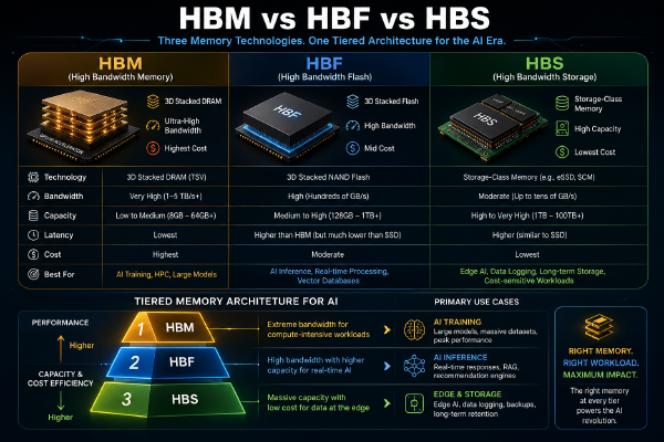
HBF is intended to occupy a new position between these two worlds.
        High-Speed Compute
               │
               ▼
              HBM
        Low Latency / Cache
               │
               ▼
              HBF
     High Capacity / High Bandwidth
               │
               ▼
         SSD / NAND Storage
      Massive Capacity / Low Cost
The objective is to add a large, high-bandwidth capacity tier without attempting to make NAND behave identically to DRAM.
⚡ How High Bandwidth Flash Works #
HBF combines two important concepts: 3D NAND density and massive parallelism.
Traditional NAND flash is already highly vertically integrated, with hundreds of storage layers stacked inside a single device.
HBF extends this density advantage by combining multiple NAND dies using advanced vertical stacking and high-density interconnect technologies.
HBM-style vertical stacking #
The first architectural principle is borrowed from HBM.
Instead of relying on a small number of externally connected memory packages, multiple dies are stacked vertically to increase integration density and shorten internal communication paths.
Conceptually:
Traditional NAND / SSD Architecture

Controller ── Channel ── NAND Package
                   │
                   └──── NAND Package
                   │
                   └──── NAND Package


HBF Architecture

       ┌───────────────┐
       │   NAND Die    │
       ├───────────────┤
       │   NAND Die    │
       ├───────────────┤
       │   NAND Die    │
       ├───────────────┤
       │   NAND Die    │
       └───────────────┘
          High-Density
         Interconnects
Vertical integration improves package density and creates the physical foundation for much wider internal data paths.
However, stacking alone does not explain HBF’s potential bandwidth.
The more significant innovation is how the NAND arrays are accessed in parallel.
Massive parallel sub-array architecture #
Traditional NAND flash is limited by the number of channels and operations that can be active simultaneously.
HBF addresses this by dividing flash storage into a much larger number of independently accessible sub-arrays.
Each sub-array can participate in parallel read and write operations.
The architectural principle is:
Traditional NAND

        Controller
            │
       Limited Channels
       ┌────┼────┐
       ▼    ▼    ▼
      Die  Die  Die


HBF

     Wide Parallel Interface
  ┌────┬────┬────┬────┬────┐
  ▼    ▼    ▼    ▼    ▼    ▼
Sub  Sub  Sub  Sub  Sub  Sub
Array Array Array Array Array
  │    │    │    │    │    │
  ▼    ▼    ▼    ▼    ▼    ▼
Parallel NAND Operations
This changes NAND from a storage medium optimized primarily around capacity and relatively coarse-grained access into a highly parallel data source.
The goal is not to achieve DRAM-like behavior in every dimension.
The goal is to exploit NAND’s enormous density while increasing parallel read throughput enough to make it useful much closer to AI compute.
📊 HBF vs HBM: Capacity for Latency #
HBF and HBM solve different problems.
HBM remains the superior technology when an accelerator requires extremely low latency, high write performance, and predictable access behavior.
HBF trades some of those characteristics for much greater capacity and potentially lower cost.
| Characteristic | HBM | HBF |
|---|---|---|
| Memory technology | DRAM | 3D NAND flash |
| Primary strength | Low latency and extreme bandwidth | High capacity and high parallel bandwidth |
| Capacity | Relatively limited | Significantly higher potential |
| Cost per GB | High | Lower potential |
| Read performance | Extremely high | Optimized for high-throughput reads |
| Write performance | Very high | More constrained |
| Write endurance | High for memory workloads | Limited relative to DRAM |
| Latency | Extremely low | Higher than HBM |
| Best AI role | Active compute and cache | Model storage and read-heavy inference |
| Replacement relationship | — | Complementary to HBM |
The distinction is critical.
HBF is not designed to replace HBM during active, latency-sensitive computation.
Instead, it can expand the amount of model data stored close to the accelerator.
🔥 Why HBF Is Well Suited to AI Inference #
AI inference is structurally different from AI training.
Training continuously updates model parameters, requiring intensive reads and writes.
Inference, by comparison, is much more read-oriented. A trained model’s parameters can be loaded and repeatedly accessed while generating outputs.
That aligns naturally with NAND’s characteristics.
Read-heavy workloads fit NAND better #
Once a model is trained, its weights are largely static during inference.
The workload becomes:
Load Model
     │
     ▼
Read Parameters
     │
     ▼
Execute Inference
     │
     ▼
Read Parameters Again
     │
     ▼
Generate Output
This pattern reduces the importance of NAND’s write limitations.
The source material cites HBF write endurance of approximately 100,000 cycles. While this is far more restrictive than conventional DRAM-style memory behavior, it can be acceptable for architectures designed around predominantly read-intensive model access.
This means software must understand the underlying memory hierarchy.
An AI runtime cannot treat HBF as unlimited, interchangeable DRAM.
Data placement policies must instead account for:
- Read frequency
- Write frequency
- Access locality
- Latency sensitivity
- Endurance
- Bandwidth requirements
🧩 The H³ Hybrid Memory Architecture #
SK Hynix has proposed a hybrid architecture that places HBM and HBF together near the GPU.
The concept is sometimes referred to as H³, representing a heterogeneous high-bandwidth memory hierarchy.
In the reported IEEE research, the architecture combines:
- Eight HBM3E stacks
- Eight HBF stacks
- Nvidia Blackwell B200-class GPU simulation
The division of responsibilities is straightforward.
                AI Accelerator
                     │
          ┌──────────┴──────────┐
          ▼                     ▼
         HBM                   HBF
   Low-Latency Tier       High-Capacity Tier
          │                     │
          ▼                     ▼
   Active Working Data      Model Parameters
   Frequently Accessed      Large Read-Heavy Data
   Latency-Critical Data    Capacity Expansion
HBM acts as the fast working-memory tier.
HBF provides a much larger pool for model weights and other read-heavy data.
The research reported up to 2.69× higher performance per unit of power consumption compared with an HBM-only configuration.
The exact performance benefit depends heavily on workload characteristics and memory-management policies, but the broader result demonstrates the potential value of heterogeneous memory systems for inference.
🏢 Data Center Inference and Edge AI #
HBF has potential applications at both ends of the AI infrastructure spectrum.
Data center capacity expansion #
In a data center, the most immediate application is expanding the memory available to AI accelerators.
Instead of requiring every model parameter to fit entirely within expensive HBM, a system could maintain the most latency-sensitive data in HBM while storing larger portions of the model in HBF.
This creates a tiered accelerator memory architecture:
GPU Compute
    │
    ▼
┌───────────────┐
│      HBM      │
│ Active / Hot  │
│     Data      │
└───────┬───────┘
        │
        ▼
┌───────────────┐
│      HBF      │
│ Model Weights │
│ Large / Warm  │
│     Data      │
└───────┬───────┘
        │
        ▼
┌───────────────┐
│ SSD / Storage │
│ Cold / Archive│
└───────────────┘
This could allow AI accelerators to access much larger models without proportionally increasing the amount of expensive HBM required per system.
Edge AI #
HBF may also be attractive for edge inference.
Edge AI often uses pre-trained models that remain relatively static while serving inference requests.
This matches HBF’s fundamental strengths:
- High read bandwidth
- Large capacity
- Lower potential cost per GB
- Lower power requirements than equivalent large memory systems
Possible use cases include:
- Edge inference servers
- AI appliances
- Robotics systems
- Autonomous systems
- Enterprise inference appliances
- Private AI deployments
The ability to keep large pre-trained models close to local compute could reduce dependence on remote cloud infrastructure.
🚧 The Engineering Challenges Behind HBF #
The HBF concept is promising, but commercializing it is far more difficult than simply stacking NAND dies.
NAND and DRAM have fundamentally different operating characteristics.
HBF must solve problems involving:
- Interconnect density
- Package thermals
- Signal integrity
- Parallel access scheduling
- Address translation
- Wear management
- Write endurance
- Error correction
- Controller design
- Memory coherency
- Software data placement
NAND addressability is fundamentally different #
One major challenge is the relatively coarse-grained nature of NAND access.
DRAM is designed for frequent random access at relatively fine granularity.
NAND flash operates around pages and erase blocks, with more complicated programming and erase behavior.
An HBF controller and software stack therefore need to bridge the gap between:
AI Accelerator Access Pattern
           │
           ▼
Fine-Grained Memory Requests
           │
           ▼
     HBF Translation Layer
           │
           ▼
Parallel NAND Sub-Arrays
           │
           ▼
Pages / Blocks / Flash Cells
The system must expose sufficient bandwidth to the accelerator while efficiently managing the underlying flash characteristics.
Write endurance requires intelligent software #
Write endurance is another fundamental constraint.
An inference architecture must avoid treating HBF as a general-purpose scratchpad for continuously changing data.
Instead, a sensible data-placement policy may look like:
Frequently Modified Data
        │
        ▼
       HBM


Frequently Read, Rarely Modified Data
        │
        ▼
       HBF


Persistent / Cold Data
        │
        ▼
    SSD / Storage
The success of HBF will therefore depend partly on AI runtimes becoming increasingly aware of heterogeneous memory tiers.
Hardware alone cannot solve the memory-wall problem.
The software stack must understand where data should reside.
📈 HBF Capacity and Bandwidth Potential #
The capacity advantage is one of HBF’s most important characteristics.
The source material describes HBF designs targeting approximately 512 GB per device, significantly exceeding the 64 GB capacity referenced for HBM4 configurations.
HBF bandwidth is also expected to be far beyond conventional SSD architectures.
Reported figures point to bandwidth exceeding 1,638 GB/s.
That does not make HBF equivalent to HBM.
Bandwidth is only one characteristic of memory performance. Latency, access granularity, write behavior, and software overhead remain equally important.
Nevertheless, the comparison illustrates why HBF is attracting attention.
Conventional SSD
      │
      │  Massive Capacity
      │  Lower Bandwidth
      ▼

      HBF
      │
      │  Massive Capacity
      │  High Parallel Bandwidth
      ▼

      HBM
      │
      │  Lower Capacity
      │  Extreme Bandwidth
      │  Ultra-Low Latency
      ▼
HBF creates a new point in the capacity-performance trade-off space.
🏭 From Research to Commercialization #
HBF development is accelerating rapidly.
SK Hynix, Samsung, and SanDisk are pursuing the technology through a combination of memory development, packaging innovation, and ecosystem collaboration.
SanDisk has indicated plans to provide HBF samples in the second half of 2026, while early HBF products targeting AI inference are expected to reach the market in 2027.
SK Hynix has also discussed releasing trial HBF products during the second half of 2026, while commercial products from major suppliers are expected to emerge around 2027.
The commercial timeline can be summarized as:
| Period | Expected Milestone |
|---|---|
| Second half of 2026 | Initial HBF samples and trial products |
| 2026 onward | Architecture validation and ecosystem development |
| Early 2027 | Initial AI inference HBF products |
| 2027 | Broader commercial HBF product introductions |
The industry is also working toward standardization.
That will be essential.
HBF cannot become a major AI infrastructure tier if every vendor implements incompatible interfaces, packaging schemes, controllers, and software stacks.
A common ecosystem will be required across:
- Memory vendors
- AI accelerator vendors
- Packaging suppliers
- Controller developers
- Server manufacturers
- AI runtime developers
🔮 HBF and the Future of Memory-Centric AI #
For years, AI accelerator development focused primarily on increasing compute throughput.
That strategy is increasingly limited by memory capacity and data movement.
A GPU cannot efficiently use its arithmetic units if model parameters cannot be delivered quickly enough.
This is why AI infrastructure is moving toward increasingly specialized memory architectures.
HBM addressed the bandwidth problem.
HBF attempts to address the capacity problem without abandoning high-bandwidth access.
The resulting future may not be defined by a single universal memory technology.
Instead, AI accelerators may use increasingly deep heterogeneous memory hierarchies:
Fastest / Most Expensive
        │
        ▼
   On-Chip SRAM
        │
        ▼
       HBM
        │
        ▼
       HBF
        │
        ▼
     SSD / NAND
        │
        ▼
Slowest / Highest Capacity
Each tier serves a different purpose.
The key challenge becomes moving the right data to the right tier at the right time.
That is the foundation of memory-centric AI.
🚀 HBF Does Not Replace HBM—It Extends AI Memory #
The most important point about High Bandwidth Flash is that it should not be viewed as a cheaper replacement for HBM.
Its purpose is different.
HBM remains essential for workloads requiring ultra-low latency, intensive writes, and maximum bandwidth close to the compute engine.
HBF targets the enormous gap between expensive accelerator memory and conventional storage.
By combining 3D NAND density with advanced stacking and massive parallelism, it could provide AI systems with a new high-capacity memory tier capable of storing much larger models near the accelerator.
For inference, that combination is particularly compelling.
Large models are predominantly read from memory, capacity requirements continue to increase, and the cost of scaling HBM indefinitely is becoming difficult to justify.
The hybrid architecture proposed by SK Hynix points toward a likely future:
HBM for speed. HBF for capacity. SSDs for persistence.
If the industry can overcome the challenges of NAND addressability, endurance, packaging, interconnects, and software management, HBF could become an important part of the AI memory hierarchy.
The memory wall is unlikely to disappear.
But HBF may add an entirely new layer to the wall—and give AI accelerators far more room to work.