3D NAND’s Three Key Technologies Beyond 300 Layers
The race to higher 3D NAND layer counts is accelerating, but layer count alone is no longer sufficient to measure the industry’s technological progress.
After crossing the 300-layer threshold, conventional vertical-stacking approaches face increasingly severe physical and economic constraints. Deeper channel structures create difficult etching and filling challenges, while additional process steps extend manufacturing cycles, increase equipment depreciation, and make yield optimization more difficult.
As a result, the next stage of 3D NAND scaling is shifting from simply adding layers toward three complementary technologies: wafer bonding, molybdenum word lines, and higher-bit-density memory cells such as QLC.
These technologies address different scaling bottlenecks. Wafer bonding changes the underlying architecture, molybdenum addresses interconnect and process limitations, and QLC increases storage density at the cell level without requiring another proportional increase in layer count.
🧭 3D NAND Scaling Has Entered a New Phase #
NAND flash initially followed the conventional semiconductor scaling model. In planar, or 2D, NAND, manufacturers continuously reduced memory-cell dimensions on the wafer surface to increase density.
That strategy eventually encountered fundamental physical and economic limits.
As cell dimensions approached the 1X-nanometer generation and below, shrinking the planar structure increasingly intensified several problems. Reduced spacing increased capacitive coupling between neighboring cells, while the smaller charge capacity of each cell made data retention and program/erase performance more difficult to balance.
At the same time, increasingly sophisticated lithography pushed manufacturing costs higher. Instead of continuously reducing cost per bit, further planar scaling risked producing the opposite result.
From planar scaling to vertical stacking #
The industry’s response was to change the scaling direction entirely.
Samsung demonstrated its V-NAND technology in 2013, followed by 32-layer products entering mass production in 2014. Instead of continuing to shrink memory cells laterally, manufacturers began stacking memory cells vertically.
This architectural transition established layer count as one of the most visible indicators of NAND technology progress.
The industry subsequently moved through generations of approximately 32, 48, 64, 96, 128, and 176 layers before broadly crossing the 200-layer threshold around 2022.
The pace has continued:
- SK hynix introduced a 321-layer 1Tb TLC product, establishing an early 300+ layer milestone.
- Its 321-layer 2Tb QLC subsequently entered mass production, marking a major step for high-density QLC NAND.
- Samsung has been developing its V10 generation toward approximately 400-layer-class NAND.
- Micron’s G9 NAND generation reaches up to 276 layers.
- Kioxia has sampled its 332-layer 10th-generation BiCS FLASH technology.
The industry’s longer-term roadmap extends considerably further.
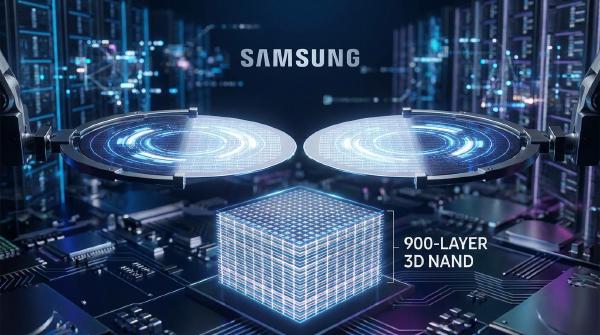
Assuming continued vertical scaling, future generations could eventually exceed 1,000 stacked word lines. Samsung previously outlined a vision for 1,000-layer 3D NAND by 2030, while Kioxia CTO Hidefumi Miyajima has indicated a goal of mass-producing NAND with more than 1,000 layers by 2031.
The important question, however, is not simply how many layers can be stacked.
It is how those layers can be manufactured economically and reliably.
🧱 Three Technologies Are Redefining 3D NAND Scaling #
Beyond approximately 300 layers, conventional scaling encounters both physical and economic headwinds.
From a physical perspective, deeper structures increase resistance, signal delay, power consumption, and manufacturing complexity. Extremely deep channel holes also make etching and filling progressively more difficult.
From an economic perspective, every additional layer can require more deposition, etching, cleaning, and other process steps. Longer cycle times, greater equipment utilization, and more complicated yield ramping can reduce the cost-per-bit benefits that originally made vertical scaling attractive.
Consequently, the industry’s competitive focus is expanding into three areas:
- Architecture: wafer bonding
- Materials: molybdenum word lines
- Cells: QLC and other multi-bit technologies
Wafer bonding is becoming the architectural foundation #
Wafer bonding separates the memory array and peripheral CMOS circuitry into independently optimized structures before combining them through high-precision bonding.
This approach allows each wafer to be manufactured using process conditions better suited to its specific function. Once bonded, the resulting structure can provide higher density and potentially improve I/O performance, manufacturing flexibility, yield management, and development efficiency.
Leading manufacturers are increasingly incorporating this strategy into advanced NAND generations.
SK hynix adopted wafer bonding in its V10 architecture, while Samsung’s V10 BV-NAND architecture also represents a move toward bonding-based approaches.
Kioxia moved earlier with its CBA (CMOS directly bonded to Array) architecture, which entered mass production with its 218-layer eighth-generation BiCS FLASH technology in 2023.
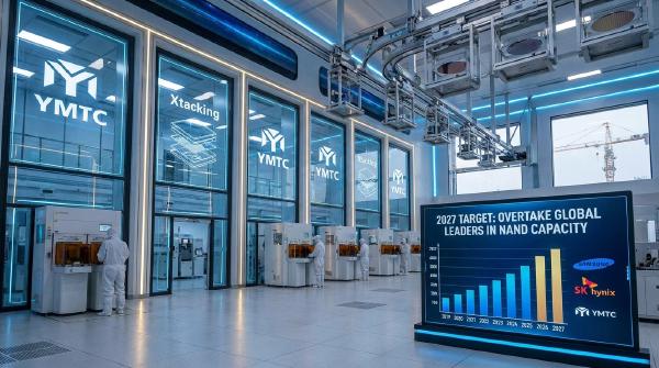
China’s YMTC has been an especially important early adopter. Its Xtacking architecture, introduced into mass production in 2018, separates the memory array and peripheral circuits before bonding them together. The architecture has since evolved through multiple generations.
The significance of wafer bonding is therefore larger than simply increasing layer count. It changes how the NAND stack is constructed and provides manufacturers with an alternative route around some of the limitations of monolithic vertical scaling.
Molybdenum addresses the word-line bottleneck #
Materials engineering is another critical component of high-layer-count NAND.
The word-line material used in 3D NAND has evolved from polysilicon to tungsten, and the industry is now moving toward molybdenum (Mo).
The transition from polysilicon to tungsten was an important step in early 3D NAND development because tungsten provided lower resistance and better electrical characteristics for increasingly tall structures.
At more than 300 layers, however, tungsten itself faces new challenges.
As dimensions shrink and aspect ratios increase, maintaining low resistance and reliably filling extremely narrow structures becomes more difficult. Molybdenum offers attractive electrical and process characteristics for these next-generation structures.
Its lower resistivity can reduce word-line resistance at comparable dimensions, potentially improving signal transmission. Its material and deposition characteristics can also provide advantages for extremely narrow features and high-aspect-ratio NAND structures.
This makes molybdenum more than a simple incremental material substitution. It is increasingly becoming part of the industry’s strategy for extending 3D NAND scaling beyond conventional tungsten-based architectures.
According to a statement attributed to SemiAnalysis, molybdenum is effectively becoming a requirement for NAND scaling beyond 300 layers rather than merely an optimization.
QLC provides another density dimension #
Layer stacking is not the only way to increase NAND density.
At the cell level, manufacturers can increase the number of bits stored in each memory cell:
- SLC: 1 bit per cell
- MLC: 2 bits per cell
- TLC: 3 bits per cell
- QLC: 4 bits per cell
Moving from TLC to QLC can increase the amount of data stored within the same physical cell area without requiring another equivalent increase in the number of vertical layers.
This becomes particularly valuable as the incremental benefits of additional layers diminish.
QLC therefore provides a second density lever that complements architectural scaling. A manufacturer can increase storage density through cell-level bit density while simultaneously developing higher-layer-count NAND.
The trade-off is that QLC introduces greater requirements for controller algorithms, error correction, endurance management, and data-retention optimization. For applications where capacity and cost per bit are more important than write endurance, however, these trade-offs can be attractive.
The growth of AI infrastructure is strengthening this demand. Increasing volumes of training data, inference data, checkpoints, and other datasets are driving demand for high-capacity storage in data centers.
This creates an increasingly important role for high-capacity QLC enterprise SSDs, particularly in workloads where storage density and total cost of ownership outweigh the endurance advantages of higher-cost alternatives.
📈 NAND Demand Is Shifting Toward Enterprise SSDs #
The technology transition is occurring alongside a major change in NAND demand.
According to Counterpoint Research data cited in the original analysis, global NAND flash revenue reached approximately $46 billion in Q1 2026, representing a substantial year-over-year increase. Enterprise SSDs (eSSDs) were identified as the primary demand driver.
Enterprise SSDs reportedly represented approximately 43% of NAND market value in Q1 2026, with the share projected to exceed 60% by the end of the year.
This demand profile is particularly important for advanced NAND manufacturers because enterprise storage places a premium on capacity, performance, power efficiency, reliability, and total cost of ownership.
As AI infrastructure expands, these requirements increasingly favor high-density NAND technologies such as advanced-layer TLC and QLC.
🏭 Which NAND Manufacturers Stand to Benefit? #
The shift beyond 300-layer NAND is also reshaping the competitive landscape.
Samsung remains the largest NAND manufacturer, while SK hynix—including Solidigm in relevant market statistics—continues to occupy the second position. Kioxia, Micron, SanDisk, and YMTC remain closely positioned in the next tier of competition.
YMTC is particularly notable in the current growth cycle.
According to the cited Counterpoint Research figures, YMTC’s revenue increased by roughly 445% year over year, while its NAND market share increased from approximately 8% to 13%.
The company’s growth illustrates how increasing domestic demand, supply constraints, and pricing improvements can rapidly change the competitive position of NAND suppliers.
However, the potential beneficiaries extend beyond NAND manufacturers themselves.
Controllers and modules #
Domestic NAND controller companies can benefit primarily from increasing shipment volumes and the continued expansion of localized supply chains.
The opportunity is therefore driven less by NAND price increases themselves and more by rising adoption, qualification, and localization of controller technologies.
For module manufacturers, the current cycle combines inventory effects with structural market consolidation.
Tight NAND supply and rising wafer and die prices can allow companies holding sufficient inventory to realize significant inventory gains. At the same time, larger module manufacturers can use stronger financing capabilities and diversified wafer procurement channels to increase their market share.
Leading suppliers are also expanding into higher-value segments such as enterprise, automotive, and industrial storage.
Smaller manufacturers without reliable access to NAND supply face greater pressure, accelerating consolidation toward larger players.
Semiconductor equipment and materials #
The longer-term opportunity may be even more significant for upstream equipment and materials suppliers.
Higher-layer-count 3D NAND requires additional process steps across:
- Etching
- Thin-film deposition
- Cleaning
- Deposition precursor materials
- Other wafer-processing operations
As vertical structures become deeper, the number and complexity of these processes increase.
Thin-film deposition provides a particularly clear example. More advanced semiconductor processes generally require additional deposition steps, while the transition from 2D to 3D NAND has also increased the proportion of manufacturing expenditure associated with deposition.
This creates a direct relationship between increasing NAND complexity and demand for process equipment.
Once domestic equipment and materials suppliers successfully complete customer qualification and production verification, they can potentially participate in recurring orders driven by both capacity expansion and technology migration.
🔭 The Next NAND Race Is About More Than Layer Count #
The semiconductor industry’s move toward 1,000-layer 3D NAND does not mean that layer count has become irrelevant. It remains a fundamental indicator of vertical scaling capability.
But after 300 layers, layer count alone provides an increasingly incomplete picture of NAND competitiveness.
The next generation of scaling depends on multiple technologies working together:
- Wafer bonding changes the architecture and separates process optimization between memory arrays and CMOS circuitry.
- Molybdenum word lines address resistance and manufacturing challenges in increasingly narrow, high-aspect-ratio structures.
- QLC increases cell-level density without requiring a proportional increase in vertical layers.
At the same time, AI-driven storage demand is changing the commercial equation. Enterprise SSDs and high-capacity QLC products are becoming increasingly important, while the expansion of advanced NAND manufacturing creates opportunities throughout the controller, module, equipment, and materials supply chains.
The industry’s next competitive phase will therefore be determined not simply by who can stack the most layers, but by who can integrate architecture, materials, cell technology, manufacturing yield, and cost efficiency into a commercially scalable NAND platform.