Samsung 900-Layer NAND: 450-Layer Wafer Bonding Explained
Samsung has developed a prototype 900-layer 3D NAND flash chip using its proprietary Cell Multi-Bonding (CMB) technology, marking a major shift in how NAND manufacturers can scale vertical memory density.
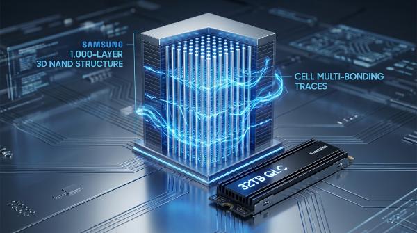
Rather than fabricating all 900 layers as a single monolithic NAND structure, Samsung’s approach bonds two independently manufactured 450-layer cell wafers into a single integrated memory structure using advanced hybrid bonding techniques.
The prototype is reportedly capable of delivering approximately 3× the storage density of current mass-production NAND, potentially providing a significant path toward higher-capacity SSDs for AI data centers, hyperscale infrastructure, enterprise storage, and eventually consumer devices.
However, the technology is not yet ready for high-volume manufacturing. Samsung is continuing to optimize the hybrid bonding process, particularly around wafer alignment, warping, yield, and manufacturing stability. As a result, commercialization of the 900-layer architecture is expected to remain several quarters away.
🚀 Samsung Pushes 3D NAND Beyond Conventional Layer Scaling #
The 900-layer NAND prototype represents a fundamentally different approach to increasing vertical NAND density.
Traditional 3D NAND scaling primarily increases the number of memory layers fabricated within a single wafer. As the layer count rises, however, increasingly deep channel etching and increasingly complex manufacturing processes create significant physical and economic constraints.
Samsung’s CMB approach attempts to bypass some of these limitations by dividing the structure into separately manufactured wafers.
Cell Multi-Bonding Combines Two 450-Layer Wafers #
The core of Samsung’s approach is Cell Multi-Bonding.
Instead of creating a 900-layer structure monolithically, Samsung manufactures two individual 450-layer NAND cell wafers and then bonds them together.
The resulting architecture provides:
- 900 total NAND layers
- Two independently manufactured 450-layer cell wafers
- Approximately 3× the storage density of current mass-production NAND, according to reported figures
- A scalable path beyond conventional single-wafer vertical stacking
This method effectively turns wafer bonding into another dimension of NAND scaling.
How Samsung’s Approach Compares With Industry NAND #
The semiconductor industry is already moving toward increasingly tall NAND structures.
SK hynix has reached a reported 321-layer 4D NAND configuration in mass production, while Samsung is preparing its 10th-generation V-NAND with more than 400 layers.
Samsung’s 900-layer CMB prototype takes a different path by combining two next-generation wafer structures rather than attempting to etch all of the layers into one wafer.
The distinction is important: the technology does not simply represent a conventional increase from 400 or 500 layers to 900 layers. It represents a change in the physical architecture used to achieve that layer count.
🔬 Hybrid Bonding Solves the Limits of Monolithic NAND #
As NAND layer counts increase, simply adding more layers to one wafer becomes increasingly difficult.
Ultra-tall monolithic NAND structures encounter multiple engineering constraints, including:
- Wafer thickness
- Wafer warping
- Vertical channel fabrication
- Thermal dissipation
- Power delivery
- Manufacturing yield
- Bonding and alignment precision
- Die size
Samsung’s Cell Multi-Bonding architecture distributes the physical structure across two wafers, potentially making it easier to overcome some of these limitations.
Embedded Metal Interconnects Enable Wafer-to-Wafer Integration #
CMB relies on advanced bonding technology in which embedded metallic interconnects allow the independently manufactured wafers to become a unified electrical structure.
The bonding process must maintain extremely high positional accuracy because even small alignment errors can prevent the corresponding electrical connections from making reliable contact.
This becomes increasingly challenging as the physical dimensions of the NAND structure expand and the wafers experience deformation during manufacturing and bonding.
Wafer Warping Is a Major Manufacturing Challenge #
One of the most difficult problems Samsung has had to address is wafer warping.
Large silicon wafers can experience physical deformation during semiconductor processing. At conventional layer counts, small deviations may be manageable, but the tolerance becomes much tighter when multiple ultra-thick NAND structures must be aligned and bonded together.
Even small amounts of deformation can introduce positional errors that affect the bonding interface.
Samsung has reportedly addressed this problem using an advanced upper chuck design that securely holds the wafers during bonding.
The system combines:
- Micron-scale chuck mechanisms
- Controlled wafer positioning
- Stack-correction algorithms
- Alignment compensation for bonding drift
These technologies are designed to maintain the required precision while compensating for physical deformation during the bonding process.
⚡ Samsung Redesigns NAND Architecture for Higher Density #
Increasing the number of memory layers is only useful if the resulting device can operate within practical power and thermal limits.
Samsung therefore redesigned several critical parts of the NAND architecture for its high-density implementation.
The objective is to increase storage capacity while avoiding a proportional increase in power consumption, die area, and thermal output.
New Bit Line and Word Line Structures #
Samsung has implemented redesigned bit line and word line structures to control power consumption and maintain manageable die dimensions.
These interconnect structures are critical because NAND scaling increases not only the physical number of memory cells but also the complexity of distributing signals and power throughout the memory array.
Optimizing the interconnect architecture therefore becomes increasingly important as vertical density rises.
A high-density NAND device that requires excessive power or generates too much heat would be difficult to deploy efficiently in large-scale storage systems.
Energy Efficiency Matters for AI Storage #
The timing of Samsung’s development is particularly relevant to the rapid growth of AI infrastructure.
AI training and inference clusters are generating enormous volumes of data, increasing demand for high-capacity enterprise SSDs and high-density storage systems.
For hyperscale data centers, storage efficiency is increasingly measured not only in capacity but also in watts per terabyte and physical storage density.
Higher-density NAND can potentially allow data centers to store more information within the same physical footprint while reducing the number of SSDs and associated infrastructure required for a given capacity target.
🏢 900-Layer NAND Targets Enterprise and AI Data Centers #
Samsung’s ultra-high-layer NAND technology is particularly relevant to storage systems where capacity density is a major constraint.
Potential target applications include:
- Enterprise SSDs
- Hyperscale data centers
- AI training infrastructure
- AI inference infrastructure
- High-capacity cloud storage
- Large-scale archival systems
AI workloads are particularly storage-intensive because modern models depend on enormous datasets, checkpoints, embeddings, logs, and generated data.
Increasing NAND density can help storage vendors build higher-capacity SSDs without proportionally increasing their physical size.
Higher NAND Density Could Increase SSD Capacity #
The practical benefit of a 900-layer NAND architecture is not simply the layer-count number itself.
More memory cells can be integrated into a smaller physical area, potentially allowing SSD manufacturers to increase capacity while maintaining familiar form factors.
For enterprise storage, this could translate into:
- Higher-capacity SSDs
- Greater storage density per rack
- Reduced physical footprint
- Lower infrastructure requirements per terabyte
- Potentially improved storage economics
The actual commercial benefits will depend on manufacturing yield, controller architecture, endurance characteristics, power consumption, and cost per bit.
🧱 Hybrid Bonding Must Mature Before Mass Production #
Despite the impressive prototype, Samsung still faces significant challenges before 900-layer NAND can enter volume production.
Hybrid bonding is considerably more demanding than conventional NAND fabrication because the bonding interface must maintain extremely high alignment precision across a large wafer area.
Manufacturing yield is another critical issue.
A defect in either of the two 450-layer wafers can potentially affect the completed bonded structure. Samsung therefore needs a process that can produce both wafer types at sufficiently high yield while maintaining consistent bonding quality.
Manufacturing Yield Will Determine Commercial Viability #
For NAND manufacturers, achieving a technically functional prototype is only the first stage.
Commercial production requires the architecture to meet stringent targets for:
- Wafer yield
- Bonding yield
- Manufacturing throughput
- Power efficiency
- Reliability
- Cost per bit
- Thermal performance
- Long-term endurance
The economic equation becomes especially important for NAND because the industry operates at extremely large production volumes.
If the additional bonding process significantly increases manufacturing costs, the higher density must generate enough value to offset that complexity.
Samsung’s ongoing process optimization will therefore be just as important as the underlying 900-layer architecture itself.
📅 Samsung’s Roadmap Toward 900-Layer and 1,000-Layer NAND #
Samsung appears to be pursuing a phased approach to commercialization.
Phase 1: 10th-Generation V-NAND #
The first step is the mass production of 10th-generation V-NAND, expected to exceed 400 layers.
This generation establishes the manufacturing foundation for Samsung’s next phase of vertical NAND scaling.
Phase 2: 900-Layer Cell Multi-Bonding #
The second stage involves commercializing the 900-layer CMB architecture.
Samsung must first improve hybrid bonding maturity, manufacturing yield, wafer alignment, and production throughput before the technology can move into high-volume manufacturing.
The 900-layer NAND architecture is therefore expected to follow the standalone 10th-generation V-NAND rather than immediately replacing it.
Mass production is currently expected to require several additional quarters of development.
🔮 Could Samsung Reach 1,000-Layer V-NAND? #
Samsung’s 900-layer prototype could represent an important stepping stone toward 1,000-layer V-NAND.
The key significance of CMB is that it changes the scaling model.
Instead of continually making a single wafer structure taller, manufacturers can potentially combine multiple independently optimized NAND structures through advanced bonding technologies.
This creates another axis for increasing storage density.
If Samsung successfully solves the manufacturing challenges associated with wafer bonding, alignment, thermal management, and yield, similar techniques could eventually enable NAND structures exceeding 1,000 layers.
The Future of NAND Scaling May Be Three-Dimensional in More Than One Sense #
The traditional definition of 3D NAND scaling focuses on stacking memory cells vertically within a single wafer.
CMB introduces another level of three-dimensional integration by stacking already-completed high-layer-count wafer structures.
That distinction could become increasingly important as conventional vertical scaling approaches its physical and economic limits.
Instead of asking only how many layers can be fabricated on one wafer, future NAND architectures may increasingly ask how many optimized memory structures can be reliably bonded together.
📈 What Samsung’s 900-Layer NAND Means for the Storage Market #
Samsung’s 900-layer NAND prototype demonstrates that the future of flash-memory scaling may depend as much on advanced packaging and hybrid bonding as on conventional transistor and memory-cell process improvements.
The architecture combines two 450-layer wafers to achieve approximately 900 layers while avoiding the need to fabricate the entire structure monolithically.
This approach could provide a path toward dramatically higher storage density while preserving practical die dimensions and power characteristics.
For AI data centers and hyperscale infrastructure, the implications are particularly significant. As AI workloads continue generating larger datasets and increasing storage requirements, higher NAND density can help operators increase capacity without proportionally increasing rack space, device count, and infrastructure overhead.
Samsung’s current prototype is still several quarters away from mass production, and its eventual commercial viability will depend heavily on bonding yield, manufacturing cost, reliability, and power efficiency.
Nevertheless, the development signals a potentially important transition in 3D NAND technology: future storage density gains may come not only from adding more layers to a wafer, but also from learning how to reliably bond entire high-layer-count NAND structures together.
If that manufacturing model proves scalable, 900-layer and eventually 1,000-layer V-NAND could become important milestones in the next generation of high-density NAND flash storage.