Huawei Tau Scaling V2 Explained: Is the Semiconductor Industry Entering the Tau Era?
For more than six decades, the semiconductor industry has been guided by a single principle: smaller process nodes mean better chips. Progress has traditionally been measured by shrinking transistors—from 90nm to 7nm, then 5nm, 3nm, and now 2nm—with each generation promising higher performance and greater efficiency.
That model is becoming increasingly difficult to sustain.
Advanced lithography has become extraordinarily expensive, leading-edge chip designs routinely cost well over $1 billion, and the historical trend of declining cost per transistor has largely stalled. As geometric scaling approaches practical and economic limits, the industry is increasingly exploring new ways to continue improving computing performance.
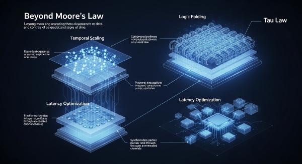
Huawei’s recently updated paper, A Time Scaling Theory for Multi-Layer Electronic Systems (Version 2), proposes one such alternative. Rather than treating transistor size as the primary measure of progress, the framework introduces Tau Scaling, a methodology that uses system latency (τ) as the common optimization target across the entire computing stack.
Whether Tau Scaling ultimately becomes an industry-wide paradigm remains uncertain, but it offers an ambitious vision for extending performance improvements beyond traditional process-node scaling.
Moving Beyond Geometric Scaling #
Conventional semiconductor development focuses on reducing physical dimensions. Smaller transistors generally allow for:
- Higher transistor density
- Lower switching power
- Faster operating frequencies
- Greater overall performance
However, modern chips increasingly encounter bottlenecks that shrinking transistors alone cannot solve.
Memory latency, interconnect delays, packaging constraints, data movement, and system-level communication have become dominant factors limiting overall performance, particularly for AI workloads.
Tau Scaling proposes shifting the optimization target from physical dimensions to time.
Instead of asking how many nanometers separate transistor gates, the framework asks a different question:
How much time does every operation require from transistor switching to application execution?
In this model, every engineering discipline contributes toward minimizing a single parameter: τ, the effective delay throughout the computing system.
What Is Tau (τ)? #
Within the proposed framework, τ represents the characteristic delay experienced as information moves through different layers of an electronic system.
Rather than existing at only one level, τ spans roughly twelve orders of magnitude.
| Layer | Primary Delay |
|---|---|
| Transistor | Switching delay (picoseconds) |
| Circuit | Signal propagation (nanoseconds) |
| Chip | Compute and memory latency (microseconds) |
| System | Network and data center communication (milliseconds to seconds) |
Historically, each engineering discipline optimized its own metrics independently.
- Process engineers focused on transistor density.
- Circuit designers optimized timing closure.
- Architects improved cache efficiency.
- System designers reduced communication overhead.
Tau Scaling attempts to unify all of these efforts under one objective:
Reduce end-to-end latency throughout the entire computing stack.
A Unified Scaling Model #
The paper introduces a generalized scaling relationship:
$$ \[ \tau_{n+1}=\frac{\tau_n}{\alpha} \] $$
where α represents the improvement factor for a given application domain.
Illustrative annual targets include:
| Application | Annual Improvement Target |
|---|---|
| Mobile devices | 1.3× |
| Autonomous driving | 1.5× |
| AI computing | Up to 10× |
Under this framework, process-node shrinkage becomes just one of many tools available for reducing latency.
Other equally important methods include:
- 3D integration
- Hybrid bonding
- Optical interconnects
- Unified memory systems
- Architectural redesign
- Software-hardware co-optimization
Rather than replacing Moore’s Law, Tau Scaling reframes transistor scaling as one contributor within a broader optimization strategy.
LogicFolding: Turning Theory into Engineering #
The paper presents LogicFolding as the practical implementation of Tau Scaling at the chip level.
Unlike traditional 3D packaging, which separates entire functional blocks onto different dies, LogicFolding proposes distributing logic at a much finer granularity.
Conventional 3D Integration #
Traditional stacking typically assigns major functional units to different layers.
For example:
- CPU
- GPU
- Memory
Each remains largely intact as a separate building block.
This approach improves package density but still limits optimization across module boundaries.
Cell-Level Optimization #
LogicFolding instead proposes distributing logic cells themselves across vertically stacked active layers.
The paper describes this transition as moving from macroblock partitioning toward continuous cell-level optimization once hybrid bonding reaches sufficiently fine interconnect pitches.
A useful analogy is comparing office buildings.
Traditional stacking places entire departments on separate floors.
LogicFolding instead distributes closely collaborating employees across multiple floors while connecting them with ultra-fast elevators, dramatically shortening communication time.
In semiconductor terms, critical logic paths can be reorganized vertically rather than remaining constrained by two-dimensional layouts.
Why Hybrid Bonding Matters #
LogicFolding relies heavily on advanced hybrid bonding.
Unlike microbump-based packaging, hybrid bonding creates extremely fine metal-to-metal connections between active silicon layers.
This enables:
- Much shorter signal paths
- Lower interconnect resistance
- Higher bandwidth
- Reduced power consumption
- Increased integration density
By reducing communication distances from millimeters to micrometers, vertical signal propagation becomes substantially faster and more energy efficient.
Kirin 2026: Reported Engineering Results #
The paper uses Huawei’s Kirin 2026 processor as an engineering demonstration of LogicFolding.
According to the published data, the design remains on the same manufacturing node as its predecessor while relying primarily on architectural changes.
Reported improvements include:
| Metric | Reported Improvement |
|---|---|
| Transistor density | +55% |
| Power consumption | -41% |
| Chip area | -37.5% |
| Power density | -5.6% |
| CPU frequency | 2.75 GHz → 3.1 GHz |
| SRAM speed | +40% |
| Routing length | -30% |
| Clock skew | -25% |
The central claim is that substantial performance and efficiency gains can be achieved without moving to a newer lithography node.
If broadly reproducible, this would represent a significant shift in how semiconductor progress is measured.
Extending Tau Scaling to AI Systems #
While LogicFolding addresses chip-level performance, the paper expands Tau Scaling to AI infrastructure through three complementary technologies.
Unified Memory Semantic Bus #
Modern AI clusters often rely on multiple communication protocols that introduce significant latency.
Huawei proposes a unified memory architecture designed to eliminate protocol conversion overhead and provide hardware-native peer-to-peer memory access.
According to the paper, remote memory access latency could decrease from tens of microseconds to roughly 100 nanoseconds.
The broader objective is to make large AI clusters behave more like a single integrated processor.
Hi-ONE Optical Interconnect #
Copper interconnects increasingly limit both bandwidth and power efficiency.
The proposed Hi-ONE architecture moves optical interfaces directly adjacent to chip packages.
Potential benefits include:
- Up to 8 Tb/s bandwidth per module
- Transmission distances extending to approximately 100 meters
- Reduced cabling complexity
- Lower transmission latency
- Improved cabinet-scale density
Optical communication becomes another mechanism for reducing system-wide τ.
Three-Dimensional System Folding #
Traditional 2.5D packaging eventually encounters what the paper describes as an edge bandwidth limitation.
As chip area grows:
- Compute capability scales approximately with area.
- Memory interfaces remain constrained along chip edges.
This mismatch increasingly limits overall system performance.
Three-dimensional system integration instead distributes memory, optical interfaces, and power delivery vertically, allowing bandwidth to scale alongside compute density.
According to Huawei, combining these approaches could increase AI hardware integration density by more than 100× by 2035.
Challenges That Remain #
The paper also acknowledges several major obstacles before Tau Scaling could become widely adopted.
New EDA Software #
Today’s electronic design automation tools are optimized primarily for planar chips.
Cell-level optimization across multiple active silicon layers would require entirely new design methodologies and software capable of optimizing directly for latency.
Process Variation #
Stacking wafers manufactured under different conditions introduces electrical variation that can affect timing accuracy and clock synchronization.
Managing these differences will require sophisticated compensation techniques.
Vertical Interconnect Trade-offs #
Although hybrid bonding reduces communication distance, additional vertical connections introduce their own resistance and capacitance.
Designers must ensure that overall latency reductions outweigh the added interconnect overhead.
Power Versus Latency #
Reducing delay alone is not sufficient.
Aggressively minimizing latency often increases power consumption.
Achieving practical systems will require balancing:
- Voltage
- Thermal management
- Optical communication
- Power delivery
- Architectural efficiency
rather than optimizing only for speed.
Looking Ahead #
Version 2 of Huawei’s Tau Scaling paper represents a notable evolution from its initial publication.
Where the original proposal primarily introduced a theoretical framework, the updated version expands substantially with engineering methodologies, implementation strategies, reported silicon data, and long-term technology roadmaps.
Whether Tau Scaling ultimately becomes a widely adopted industry standard remains an open question. The semiconductor ecosystem has historically required broad participation from foundries, EDA vendors, equipment manufacturers, packaging specialists, and system architects before new scaling paradigms become mainstream.
Even so, the paper reflects a broader trend already visible across the industry: as conventional transistor scaling delivers diminishing returns, future performance improvements are increasingly expected to come from system-level optimization, advanced packaging, heterogeneous integration, and three-dimensional architectures.
In that context, Tau Scaling is less about replacing Moore’s Law than expanding the definition of semiconductor progress. As physical shrinkage approaches practical limits, reducing latency throughout the entire computing stack may become one of the industry’s most important avenues for future innovation.