IMEC Roadmap: Sub-1nm Chips Expected Around 2034
Recent discussions surrounding 2nm manufacturing and experimental 1.4nm technologies have led many consumers to believe that sub-1nm processors are just around the corner.
However, the latest long-term semiconductor roadmap released by IMEC — the world’s leading nanoelectronics research center — paints a far more realistic picture of process evolution over the next two decades.
According to the roadmap, true sub-1nm semiconductor technology is unlikely to arrive before 2034, while Moore’s Law itself may continue for another 20 years through architectural innovation, new materials, and advanced transistor structures.
The roadmap provides one of the clearest public views yet into the future direction of semiconductor scaling from 2020 through 2046.
🧩 IMEC Clarifies the Future of Moore’s Law #
For years, the semiconductor industry maintained extremely aggressive density scaling.
Between 1998 and 2010:
- Logic chip density increased by roughly 50% annually
- SRAM cell area regularly halved
- Performance-per-watt improved rapidly
However, from 2010 onward, scaling efficiency began slowing significantly as transistor miniaturization approached physical limitations.
This slowdown led many observers to claim that Moore’s Law was effectively dead.
IMEC’s roadmap suggests otherwise.
Instead of ending entirely, Moore’s Law is transitioning into a slower but still sustainable phase driven by:
- New transistor architectures
- Vertical device stacking
- Advanced materials
- Packaging innovation
- Heterogeneous integration
The result is continued density growth, albeit at a more gradual pace than during the golden era of planar transistor scaling.
⚙️ GAA Nanosheets Will Continue Until 2031 #
According to the roadmap, semiconductor manufacturers will continue relying on Gate-All-Around (GAA) nanosheet transistor technology through the early 2030s.
The roadmap projects:
| Year | Process Node | Architecture |
|---|---|---|
| Current | 2nm-class | GAA nanosheet |
| 2031 | A10 (1nm) | Final nanosheet generation |
The A10 node, expected around 2031, will represent the final major iteration of the current nanosheet transistor era.
GAA transistors already represent a major transition away from traditional FinFET structures by surrounding the transistor channel from all sides, improving:
- Electrostatic control
- Leakage reduction
- Switching efficiency
- Power characteristics
This architecture is expected to dominate advanced logic manufacturing for the rest of the decade.
🏗️ Sub-1nm Era Begins With CFET Architecture #
The roadmap indicates that the first true sub-1nm process node will arrive around 2034 through the adoption of CFET technology.
A7 (0.7nm) Node #
Projected timeline:
2034Technology transition:
CFET (Complementary Field-Effect Transistor)Unlike conventional nanosheet layouts, CFET structures vertically stack NMOS and PMOS transistors, dramatically improving density efficiency.
Potential benefits include:
- Smaller standard cell area
- Higher transistor density
- Better scaling efficiency
- Reduced interconnect distance
- Improved power efficiency
IMEC estimates CFET could improve transistor density by up to:
80%compared with standard nanosheet implementations.
This marks one of the most important architectural shifts in semiconductor manufacturing since the FinFET transition.
🔬 Roadmap Extends Toward 0.3nm and Beyond #
IMEC’s long-term roadmap extends well beyond the first sub-1nm generation.
Projected milestones include:
| Year | Node | Technology Direction |
|---|---|---|
| 2034 | A7 (0.7nm) | CFET |
| 2036 | A5 (0.5nm) | Advanced CFET |
| 2040 | A3 (0.3nm) | Further scaling |
| 2043 | A2 (0.2nm) | 2D material FETs |
| 2046 | Sub-0.2nm | Next-generation architectures |
The roadmap also suggests that entirely new material systems will eventually be required.
Future technologies may include:
- 2D semiconductors
- Atomic-layer materials
- Novel gate dielectrics
- Alternative channel structures
- Advanced backside power delivery
At these scales, conventional silicon-based scaling alone becomes increasingly difficult.
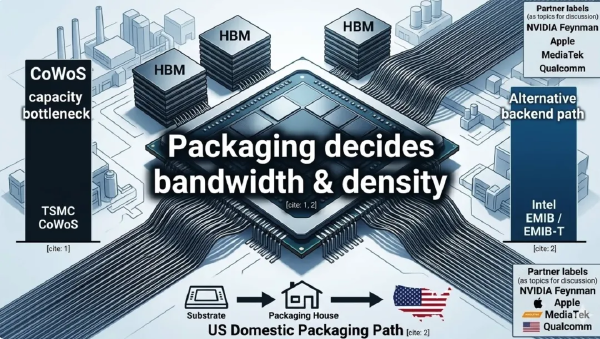
📦 Advanced Packaging Is Not a Replacement for Node Scaling #
As advanced packaging technologies continue maturing, some analysts have argued that traditional node scaling is becoming less important.
Technologies such as:
- Chiplets
- 2.5D packaging
- 3D stacking
- SiP (System-in-Package)
- Wafer-Level Packaging (WLP)
have enabled substantial gains in compute density and product flexibility.
However, IMEC’s roadmap reinforces an important industry reality:
Advanced packaging complements process scaling — it does not replace it.Packaging improvements alone cannot fully solve:
- Power efficiency limitations
- Thermal density challenges
- Memory latency constraints
- Interconnect overhead
- Energy-per-operation scaling
The underlying process node of each chiplet still fundamentally determines the system’s efficiency ceiling.
🤖 AI Workloads Continue Driving Process Innovation #
One major reason semiconductor scaling remains essential is the explosive growth of AI compute demand.
Large-scale AI workloads continue increasing at extraordinary rates, placing enormous pressure on:
- Power consumption
- Datacenter density
- Thermal management
- Interconnect bandwidth
- Performance-per-watt
Without continued transistor-level improvements, future AI infrastructure would become economically and thermally unsustainable.
This is why the industry continues investing aggressively in:
- New transistor structures
- EUV lithography
- High-NA EUV
- Advanced packaging
- Novel materials research
Even incremental node improvements now carry massive strategic value.
💡 Consumers Do Not Need to Chase Every New Node #
Despite constant marketing surrounding advanced process nodes, mainstream consumers do not necessarily benefit from immediately adopting the newest semiconductor generation.
For the next five to six years, most consumer processors will remain within the:
2nm → 1.4nmrange using GAA nanosheet architectures.
As yields mature, these products will gradually become:
- More affordable
- More power efficient
- Better optimized
- Thermally refined
Early-generation products on brand-new nodes typically carry:
- Higher pricing
- Lower initial yields
- Limited availability
- Conservative clock behavior
Waiting for process maturity often provides better overall value for mainstream buyers.
🔮 Moore’s Law Is Slowing — Not Ending #
The broader takeaway from IMEC’s roadmap is that Moore’s Law is evolving rather than disappearing.
The historical era of rapid annual scaling has unquestionably slowed. However, semiconductor innovation continues through a combination of:
- Architectural redesign
- Vertical stacking
- Material science breakthroughs
- Advanced lithography
- Heterogeneous integration
- Packaging innovation
Instead of relying on a single scaling mechanism, future progress will increasingly depend on multiple technologies advancing simultaneously.
🚀 The Semiconductor Industry Still Has a Long Runway #
If IMEC’s roadmap proves accurate, the semiconductor industry may still have another two decades of meaningful scaling ahead.
That would provide a foundation for continued growth across:
- Artificial intelligence
- High-performance computing
- Consumer electronics
- Automotive systems
- Robotics
- Edge computing
- Scientific simulation
Rather than reaching an abrupt endpoint, Moore’s Law appears to be transitioning into a more complex, multidisciplinary engineering era.
The pace may be slower than before, but semiconductor advancement is far from over.
📌 Final Thoughts #
The latest IMEC roadmap offers one of the clearest long-term views yet into the future of semiconductor manufacturing.
Key takeaways include:
- Sub-1nm technology is unlikely before 2034
- GAA nanosheets will dominate through 2031
- CFET architecture will power the first 0.7nm-class nodes
- Advanced packaging supports — but cannot replace — node scaling
- Moore’s Law can continue for another 20 years through innovation
Most importantly, the roadmap highlights that future semiconductor progress will increasingly rely on the convergence of:
- transistor architecture
- materials science
- lithography
- packaging technology
- system-level integration
The era of easy transistor scaling may be over, but the era of semiconductor innovation is still accelerating.