Intel 14A vs. 18A: Process Roadmap and Advanced Packaging
Intel Foundry used its 2025 Direct Connect event, held in San Jose, California, on April 29, 2025, to outline its next-generation semiconductor manufacturing strategy. The event highlighted Intel’s progress in advanced process technology, heterogeneous integration, advanced packaging, and foundry ecosystem development.
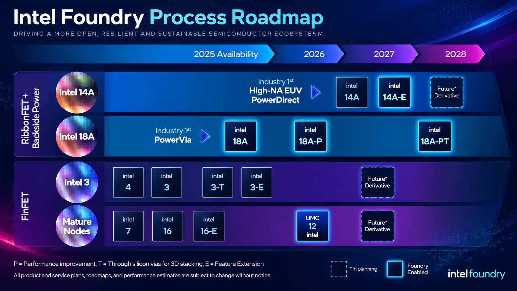
One of the most important announcements was Intel 14A, the successor to Intel 18A. Intel also introduced additional 18A derivatives, including 18A-P and 18A-PT, designed to address different performance and advanced integration requirements.
Led by Intel CEO Lip-Bu Tan, who officially took the position in March 2025, the event emphasized a broader transformation of Intel Foundry. The company aims to compete not only through transistor scaling but also through advanced packaging, manufacturing capacity, and closer collaboration with external customers.
The Intel 14A roadmap introduces several important technologies, including second-generation RibbonFET gate-all-around transistors, PowerDirect backside power delivery, and High Numerical Aperture Extreme Ultraviolet (High-NA EUV) lithography.
Meanwhile, Intel’s 18A process family is being expanded with performance-oriented and 3D-integration-focused variants.
Beyond transistor technology, Intel also presented advances in EMIB and Foveros packaging, highlighting the growing importance of chiplet integration in high-performance computing (HPC), AI accelerators, and data center processors.
Together, these developments represent Intel’s attempt to rebuild its manufacturing competitiveness and establish Intel Foundry as a more attractive alternative to TSMC and Samsung.
🚀 Intel 14A: The Successor to Intel 18A #
Intel 14A was one of the central announcements at Direct Connect 2025. As the next major generation following Intel 18A, it introduces improvements across transistor architecture, backside power delivery, and lithography.
At the event, Intel confirmed that it had engaged lead customers on 14A and distributed an early version of its Process Design Kit (PDK). Several potential customers had also expressed interest in developing test chips using the new process.
This early engagement is important because it allows external chip designers to evaluate the manufacturing technology and provide feedback before committing complete production designs.
1. PowerDirect: Second-Generation Backside Power Delivery #
One of Intel 14A’s most significant innovations is PowerDirect, an enhanced backside power-delivery technology building on the PowerVia architecture introduced with Intel 18A.
Traditional semiconductor processes generally distribute power and signals through the same frontside interconnect structure.
As transistor density increases, these interconnect networks become increasingly complicated. Power delivery competes with signal routing for limited metal-layer resources, potentially increasing resistance, voltage drop, and routing congestion.
Backside power delivery addresses this problem by moving power-distribution networks to the back of the silicon wafer.
This provides several architectural advantages:
- Frees frontside metal layers for signal routing.
- Reduces power-distribution congestion.
- Helps minimize voltage drop across power networks.
- Improves routing flexibility.
- Provides additional opportunities for transistor-density scaling.
PowerDirect advances this approach through an updated direct-contact power-delivery architecture.
By improving the connection between backside power distribution and the transistor-level power network, Intel aims to reduce delivery losses and improve overall power efficiency.
Compared with conventional frontside power delivery, the combination of backside power delivery and optimized transistor integration provides a more flexible foundation for future high-density chips.
2. High-NA EUV Lithography #
Intel 14A is also positioned as one of the first semiconductor manufacturing processes to incorporate ASML’s High-NA EUV lithography technology into advanced logic manufacturing.
High-NA EUV increases the numerical aperture of the lithography optical system, improving resolution and enabling more advanced patterning capabilities.
Compared with conventional EUV systems, High-NA EUV offers several potential benefits:
- Improved lithographic resolution.
- Greater patterning capability for advanced features.
- Potential reduction in complex multi-patterning steps.
- Better support for future transistor-density scaling.
However, High-NA EUV systems are considerably more expensive and introduce additional process-integration challenges.
Intel’s strategy is to use an appropriate combination of High-NA and conventional EUV lithography, selecting the technology for each layer according to its resolution requirements, manufacturing cost, and production efficiency.
This approach is intended to balance lithographic precision with economically viable wafer manufacturing.
3. RibbonFET 2: Second-Generation Gate-All-Around Transistors #
Intel 14A continues the company’s transition from FinFET transistors to Gate-All-Around (GAA) transistor architecture.
The process introduces RibbonFET 2, the second generation of Intel’s RibbonFET technology.
Traditional FinFET transistors use a three-dimensional fin structure with the gate controlling the channel from multiple sides.
GAA transistors extend this concept by allowing the gate to surround the channel more completely.
Intel’s RibbonFET architecture uses nanosheet-like semiconductor channels, providing improved electrostatic control and flexibility in transistor design.
The second-generation implementation is intended to improve:
- Drive-current characteristics.
- Leakage-current control.
- Transistor density.
- Power efficiency.
- Performance scaling.
Combining RibbonFET 2 with PowerDirect creates the transistor and power-delivery foundation of Intel 14A.
4. Intel 14A Performance Targets #
Intel’s published projections indicate that 14A is designed to deliver substantial improvements over 18A.
The announced targets include:
| Metric | Intel 14A Target vs. Intel 18A |
|---|---|
| Performance at the same power | 15–20% improvement |
| Power at the same performance | 25–35% reduction |
| Chip density | Up to 1.3x |
These figures represent Intel’s process-level targets rather than independently measured performance results from commercial 14A products.
Actual benefits will depend on transistor implementation, standard-cell libraries, operating voltage, chip architecture, and design characteristics.
Nevertheless, these projections illustrate Intel’s intended direction: achieving higher performance and greater integration density without proportionally increasing power consumption.
🧱 Intel 18A: Expanding the Process Family With 18A-P and 18A-PT #
Alongside Intel 14A, Intel introduced two important derivatives of its 18A manufacturing technology: 18A-P and 18A-PT.
Rather than relying on a single process configuration for every application, Intel is developing different variants to address performance and heterogeneous-integration requirements.
1. Intel 18A-P: Performance-Oriented Process Technology #
Intel 18A-P is designed to provide enhanced performance compared with the original 18A process.
The primary objective is to offer additional performance and power-efficiency optimization for customers developing high-performance computing and client processors.
Potential applications include:
- High-performance CPUs.
- AI processors.
- Client computing platforms.
- Data center compute tiles.
- Custom ASIC designs.
By extending the 18A platform, Intel can provide customers with another process option without requiring an entirely new manufacturing architecture.
This is particularly relevant for external foundry customers that need different performance and power characteristics for their products.
2. Intel 18A-PT: Enabling Advanced 3D Integration #
Intel 18A-PT introduces additional capabilities for three-dimensional integration, including through-silicon vias (TSVs).
TSVs are vertical electrical connections that pass through silicon dies or interposer structures, allowing signals and power to move between different layers of a semiconductor package.
This technology is particularly useful for advanced packaging architectures that stack multiple dies vertically.
Intel’s 18A-PT roadmap therefore supports more sophisticated heterogeneous integration involving:
- Multiple logic dies.
- Cache and memory structures.
- Compute chiplets.
- Vertical die-to-die connections.
- High-density 3D packaging.
This development is important for future server processors and AI accelerators, where performance increasingly depends on efficient communication between multiple silicon components rather than simply maximizing the capabilities of a single monolithic die.
3. Clearwater Forest and the 18A Platform #
Intel’s Clearwater Forest Xeon processor family is an important example of its transition toward advanced multi-die server architectures.
The broader 18A platform combines next-generation transistor technology with advanced packaging techniques to improve compute density and power efficiency.
The introduction of 18A-PT also illustrates why process technology and packaging technology must be developed together.
For modern data center processors, increasing transistor density is only part of the challenge. Moving data efficiently between compute tiles, cache structures, and memory is equally important.
For additional context on Intel’s 18A implementation in client processors, see Intel Panther Lake: 18A Process Powers Next-Generation Mobile CPUs.
4. Intel 18A Manufacturing and Customer Enablement #
At Direct Connect 2025, Intel confirmed that 18A had entered risk production and was expected to reach high-volume manufacturing later in 2025.
The first major products planned for the process included:
- Panther Lake client processors.
- Clearwater Forest server processors.
Intel also highlighted the release of version 1.0 of its 18A Process Design Kit to customers.
PDK availability is a critical milestone because semiconductor designers require stable design rules, process models, and verification tools before committing their chips to manufacturing.
Intel expected external customers to complete their initial 18A chip tape-outs during the first half of 2025.
These activities were intended to demonstrate that 18A could support not only Intel’s own products but also the requirements of external foundry customers.
📦 Intel Advanced Packaging: EMIB, Foveros, and 3.5D Integration #
Advanced packaging was another major focus of Intel Foundry Direct Connect 2025.
As semiconductor scaling becomes increasingly expensive, chiplet architectures and heterogeneous integration are becoming essential for building complex processors.
Instead of placing every function on a single monolithic die, manufacturers can combine multiple smaller dies built using different process technologies.
Intel has developed several packaging technologies to support this approach, including EMIB, Foveros, and Foveros Direct.
1. EMIB: Embedded Multi-Die Interconnect Bridge #
EMIB (Embedded Multi-Die Interconnect Bridge) is Intel’s 2.5D packaging technology.
It uses a small silicon bridge embedded within the package substrate to provide high-density electrical connections between adjacent dies.
Unlike traditional silicon-interposer solutions, EMIB does not require a large full-area silicon interposer covering the entire package.
This can reduce packaging complexity while maintaining high-bandwidth communication between chiplets.
EMIB has been in production since 2017 and has become an important part of Intel’s heterogeneous-integration strategy.
Its applications include:
- Multi-die processors.
- High-bandwidth memory integration.
- Data center GPUs.
- High-performance computing systems.
- Chiplet-based ASICs.
2. EMIB-T: Enhanced Interconnect and Power Delivery #
Intel also introduced EMIB-T, an enhanced version of its embedded bridge technology.
The updated architecture incorporates through-silicon vias (TSVs), providing additional flexibility for vertical connectivity and power-delivery integration.
This helps address the increasingly demanding electrical requirements of advanced multi-die packages.
As packages integrate more compute tiles and HBM stacks, power distribution and signal integrity become critical engineering challenges.
EMIB-T is intended to provide a more flexible foundation for large-scale heterogeneous integration.
3. Foveros: 2.5D and 3D Packaging Solutions #
Intel’s Foveros family covers multiple packaging configurations designed for different performance, density, and cost requirements.
The broader technology portfolio includes silicon-based interposer structures, redistribution-layer implementations, and bridge-based approaches.
Foveros-S uses a silicon interposer architecture for high-density connections, while the Foveros-R and Foveros-B variants are designed around different redistribution-layer and bridge-based integration approaches.
At Direct Connect 2025, Intel outlined plans for additional Foveros variants, with production targeted for 2027.
The goal is to expand the range of packaging options available to customers developing increasingly complex chiplet-based designs.
4. Foveros Direct 3D: Copper-to-Copper Hybrid Bonding #
Foveros Direct represents Intel’s more advanced 3D integration technology.
It uses direct copper-to-copper hybrid bonding to establish dense electrical connections between vertically stacked dies.
Compared with conventional micro-bump-based stacking, hybrid bonding enables much finer interconnect pitches and shorter electrical connection paths.
This can provide several advantages:
- Higher interconnect density.
- Lower interconnect resistance.
- Reduced communication energy.
- Greater vertical integration flexibility.
- Improved bandwidth between stacked dies.
These characteristics make Foveros Direct particularly relevant to future HPC processors and AI accelerators.
5. EMIB 3.5D: Combining Horizontal and Vertical Integration #
Intel also presented EMIB 3.5D packaging, which combines EMIB and Foveros technologies.
The idea is to support both horizontal chiplet connections and vertical die stacking within a single package.
This allows designers to integrate multiple compute tiles, memory components, and specialized silicon functions into a more complex heterogeneous system.
A representative example of Intel’s advanced integration capabilities is the Data Center GPU Max series, based on the Ponte Vecchio architecture.
The product integrates:
- More than 100 billion transistors.
- 47 active tiles.
- Five different manufacturing process technologies.
This demonstrates the complexity that can be achieved through advanced chiplet integration.
🤝 Intel Foundry Ecosystem: EDA, IP, and External Customers #
Leading-edge semiconductor manufacturing requires much more than a competitive process node.
Foundry customers also need mature electronic design automation (EDA) tools, validated intellectual property, reference design flows, and reliable manufacturing support.
Intel is therefore expanding its ecosystem partnerships to improve the accessibility of its 18A and 14A processes.
1. EDA and IP Ecosystem Partnerships #
Intel is working with major EDA and semiconductor IP providers, including:
- Synopsys.
- Cadence.
- Siemens EDA.
- Ansys.
These companies provide essential technologies for semiconductor design, simulation, physical verification, and manufacturing preparation.
Their tools need to support Intel’s manufacturing design rules and process models to ensure that customers can develop and validate chip designs efficiently.
EDA enablement and IP availability are particularly important for external customers because they reduce the engineering effort required to adopt a new foundry process.
2. Intel and Arm Emerging Businesses Initiative #
Intel has also partnered with Arm on an initiative designed to support emerging semiconductor companies.
The Emerging Businesses Initiative aims to help startups developing Arm-based system-on-chips (SoCs) access:
- Foundry manufacturing capabilities.
- Arm IP and architectural resources.
- Design ecosystem support.
- Technical collaboration.
- Potential financial assistance.
This is strategically important because many emerging chip companies do not have the resources required to independently establish a complete semiconductor design and manufacturing ecosystem.
By lowering some of these barriers, Intel hopes to attract more customers to its foundry platform.
3. External Customer Interest in Intel 18A #
Intel also highlighted interest from companies exploring its 18A manufacturing technology.
Potential customers and ecosystem participants mentioned in the broader foundry discussion included Microsoft, NVIDIA, Broadcom, and Faraday.
Microsoft was particularly notable because it planned to use Intel manufacturing capabilities for internally designed chips.
However, customer discussions, technology evaluations, test-chip programs, tape-outs, and confirmed high-volume manufacturing agreements represent different levels of commercial commitment.
The existence of customer interest should not automatically be interpreted as a confirmed production order.
For Intel Foundry, the next challenge is converting early technical engagement into long-term manufacturing partnerships and sustainable wafer demand.
⚔️ Intel 18A and 14A vs. TSMC: Process Technology Competition #
Intel’s foundry strategy is closely tied to its effort to compete with TSMC and Samsung in advanced semiconductor manufacturing.
Intel 18A and 14A are positioned as important alternatives for customers seeking leading-edge manufacturing capabilities.
1. Intel 18A vs. TSMC N2 #
Intel 18A competes in the same broad advanced manufacturing generation as TSMC’s N2 process.
One of Intel’s main differentiators is the combination of:
- RibbonFET gate-all-around transistors.
- PowerVia backside power delivery.
- Advanced multi-die packaging.
- A vertically integrated design and manufacturing ecosystem.
TSMC’s N2 process represents its transition to GAA transistor architecture.
However, the two manufacturers use different transistor implementations, design rules, libraries, and manufacturing methodologies.
Therefore, comparing them using nominal process-node names alone is not meaningful.
The relevant metrics include transistor density, performance at a given power level, power consumption at a given performance target, manufacturing yield, and production cost.
2. Backside Power Delivery as a Competitive Advantage #
Intel’s early adoption of PowerVia on 18A was an important part of its competitive positioning.
Separating power delivery from frontside signal routing provides additional flexibility for increasingly dense logic designs.
Intel 14A advances this strategy through PowerDirect.
TSMC has also been developing backside power-delivery technology, including its Super Power Rail architecture for the A16 process.
Consequently, the competitive comparison is not simply whether one manufacturer has backside power delivery and the other does not.
The more meaningful question is how effectively each company implements the technology in production, including its impact on transistor density, signal routing, power efficiency, manufacturing yield, and total design cost.
3. Intel 14A and the Next Foundry Generation #
With Intel 14A, Intel is attempting to extend its process differentiation through three major technologies:
- RibbonFET 2 transistor architecture.
- PowerDirect backside power delivery.
- High-NA EUV lithography.
The company also outlined an enhanced derivative, Intel 14A-E, on its manufacturing roadmap.
According to Intel’s 2025 roadmap presentation, 14A-E was planned as a subsequent process refinement for 2027.
The objective is to provide additional performance and power-efficiency improvements while extending the capabilities of the initial 14A platform.
However, Intel’s process roadmap and TSMC’s roadmap should be compared through actual manufacturing capabilities and commercial product performance rather than assuming that similarly numbered nodes provide equivalent transistor dimensions or density.
❄️ Future Technologies: Liquid Cooling and Glass Substrates #
Beyond transistor technology and chiplet packaging, Intel is also exploring new technologies to address the thermal and electrical challenges of future semiconductor systems.
1. Immersion Liquid Cooling for High-Power Chips #
As AI accelerators and HPC processors become increasingly powerful, thermal management is becoming a major system-design challenge.
Traditional air cooling is approaching practical limitations for extremely high-power semiconductor packages.
Intel is therefore exploring immersion liquid cooling and other advanced thermal-management technologies.
The company’s long-term research direction includes supporting chips with power requirements approaching 2,000W by 2030.
This is an ambitious future target rather than a description of currently shipping processor configurations.
Higher-power chips require more than improved cooling hardware. Package design, thermal-interface materials, power delivery, substrate construction, and system-level fluid management must also evolve.
2. Glass Substrates for Advanced Packaging #
Intel is also developing glass substrate technology, with a target introduction around 2027.
Traditional organic substrates face physical and electrical limitations as package dimensions and interconnect densities increase.
Glass offers several potential advantages:
- Better dimensional stability.
- Improved thermal and mechanical characteristics.
- Potentially lower signal loss.
- More precise high-density interconnect formation.
- Better support for large chiplet-based packages.
These properties could make glass substrates attractive for future HPC and AI packages.
As chiplet architectures continue growing in complexity, substrate technology will become increasingly important for maintaining signal integrity and package reliability.
🏭 Intel Foundry’s Long-Term Strategy Toward 2030 #
Intel Foundry Direct Connect 2025 demonstrated that the company’s manufacturing strategy extends beyond individual process nodes.
Intel aims to establish a complete foundry ecosystem combining:
- Advanced transistor manufacturing.
- Backside power delivery.
- High-NA EUV lithography.
- Advanced 2.5D and 3D packaging.
- Global manufacturing capacity.
- EDA and IP partnerships.
- External customer design support.
Intel has outlined an ambition to become the world’s second-largest foundry by 2030.
Achieving this objective will require substantial improvements in both technology execution and commercial adoption.
The company must demonstrate that its advanced processes can deliver competitive manufacturing yields, reliable production schedules, and economically attractive wafer pricing.
It must also convince external customers that Intel Foundry can provide a stable long-term manufacturing partnership.
The success of 18A and 14A will therefore influence more than Intel’s internal processor roadmap. These processes are also central to the company’s attempt to establish itself as a major external semiconductor manufacturing provider.
🧭 Conclusion: Intel Is Rebuilding Its Foundry Strategy Around Process and Packaging Innovation #
Intel Foundry Direct Connect 2025 presented an ambitious technology roadmap centered on Intel 14A, the expanding 18A process family, and advanced packaging.
Intel 14A introduces RibbonFET 2, PowerDirect backside power delivery, and High-NA EUV lithography, with the objective of improving performance, power efficiency, and transistor density over 18A.
Meanwhile, 18A-P and 18A-PT expand the manufacturing platform to address performance-oriented and advanced 3D-integration requirements.
In packaging, EMIB, EMIB-T, Foveros Direct, and EMIB 3.5D demonstrate Intel’s focus on heterogeneous integration and chiplet-based computing.
The company’s ecosystem investments in EDA tools, semiconductor IP, and partnerships with Arm and external customers are equally important because competitive process technology alone is insufficient to build a successful foundry business.
However, several challenges remain:
- Achieving consistent manufacturing yields.
- Scaling production capacity.
- Converting customer interest into confirmed production commitments.
- Maintaining competitive process economics.
- Delivering reliable advanced packaging at high volume.
- Competing with the established manufacturing ecosystems of TSMC and Samsung.
Intel’s long-term foundry ambitions will ultimately depend on execution rather than roadmap announcements. If the company can successfully commercialize 18A and 14A while scaling its advanced packaging technologies, it could become a more significant alternative in the global semiconductor manufacturing industry.
Direct Connect 2025 provided a detailed look at that strategy. The next decisive milestone will be demonstrating that these technologies can move from engineering roadmaps into reliable, commercially competitive products.