
TinyGPU v2.0: Solo Developer Achieves First-Pass GPU Tapeout
TinyGPU v2.0 has achieved something exceptionally uncommon in hardware development: a GPU designed by a single developer reached working silicon on its first tapeout attempt.
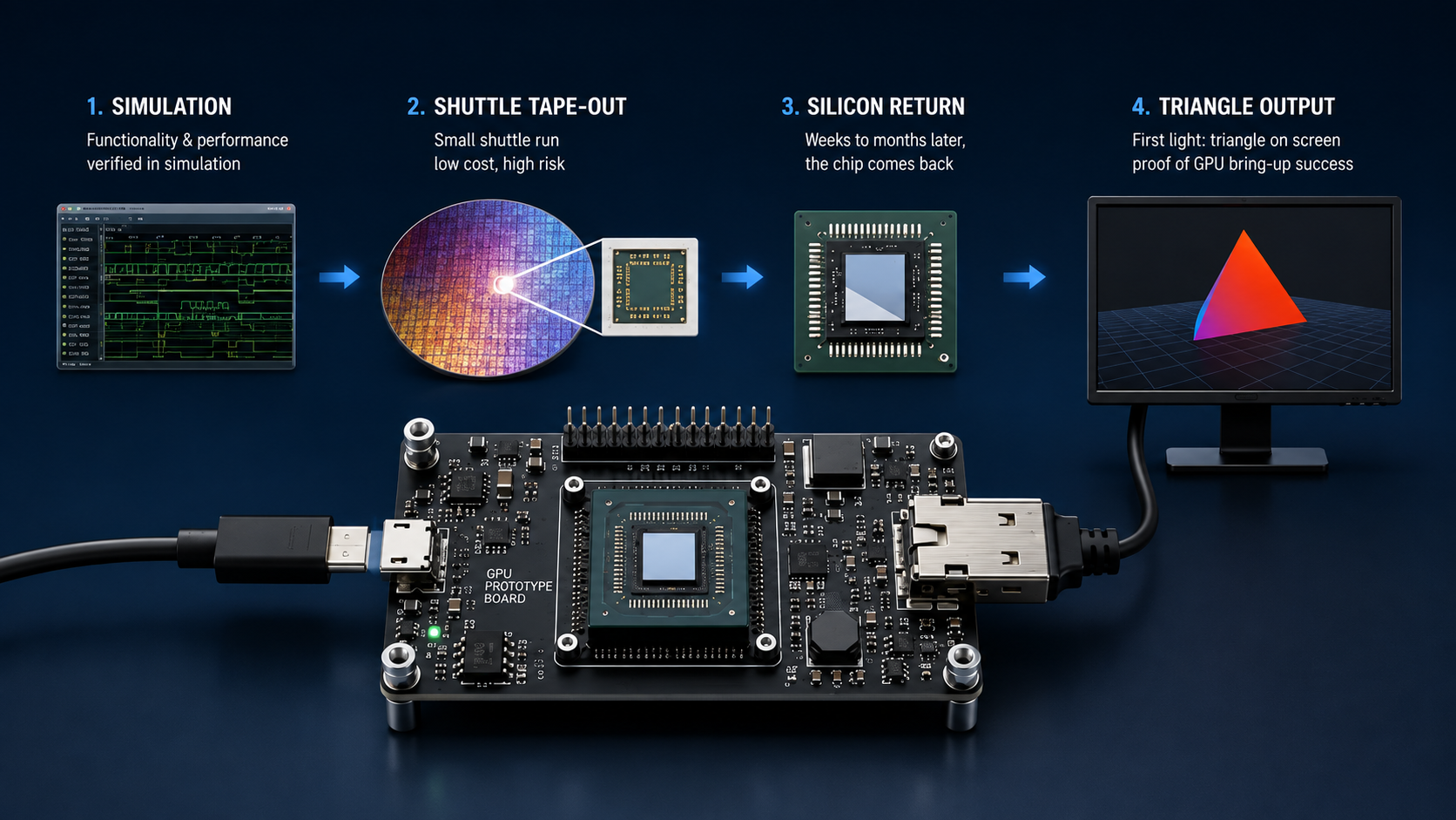
Fabricated through the Tiny Tapeout ecosystem, the chip implements a compact fixed-function 3D graphics pipeline using approximately 240,000 transistors. Despite its extremely limited hardware budget, it supports transformation and lighting, rasterization, backface culling, depth testing, flat shading, and video output.
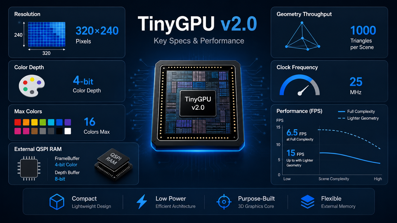
The resulting silicon operates at 25 MHz and can render simple scenes at up to 15 FPS, with heavily loaded scenes reaching approximately 6.5 FPS.
The performance is not the primary achievement. The more important result is that a complete graphics pipeline can now be inspected, modified, fabricated, and tested as open-source silicon by an individual developer.
🧩 A Complete 3D Pipeline in Just 240,000 Transistors #
TinyGPU v2.0 is a hobbyist-oriented ASIC fabricated through the SKY25b shared-mask shuttle run on Tiny Tapeout.
The multi-project wafer model is critical to projects of this scale because it distributes fabrication costs across many designs. Instead of requiring the six-figure budgets normally associated with custom silicon, individual developers can participate in shared fabrication runs at substantially lower cost.
The resulting GPU occupies a 4×4 tile footprint and implements a complete fixed-function graphics pipeline.
Its hardware includes:
- Transformation and Lighting (T&L)
- Triangle rasterization
- Backface culling
- Depth testing
- Flat shading
- A dynamic directional light
- External framebuffer and Z-buffer memory interfaces
- Video output
The design supports scenes containing up to 1,000 triangles and produces output at 320×240 resolution with 4-bit color, allowing up to 16 simultaneous colors.
A GeForce 256-Inspired Architecture #
The architectural comparison with the original GeForce 256 is particularly interesting.
NVIDIA’s GeForce 256 launched in 1999 with approximately 23 million transistors and helped establish the term “GPU” for graphics processors incorporating hardware transformation and lighting.
TinyGPU implements a broadly comparable fixed-function graphics feature set with only about 240,000 transistors—roughly 1% of the GeForce 256’s transistor count.
This does not mean the two chips offer remotely comparable performance. TinyGPU has vastly lower clock frequency, memory bandwidth, rendering resolution, color depth, and overall computational resources.
The comparison instead illustrates how much graphics functionality can be expressed in a compact hardware design when modern development tools and highly constrained requirements are used.
🎮 Working Silicon Demonstrates the Entire Graphics Path #
TinyGPU v2.0 runs at 25 MHz and relies on external QSPI RAM because its small die footprint does not provide enough area for integrated framebuffer storage.
The double buffer and 8-bit Z-buffer therefore reside in external memory.
Under maximum scene complexity, the GPU reaches approximately 6.5 FPS. With fewer geometric primitives, performance can increase to around 15 FPS.
The developer has demonstrated real-time model rotation using a gamepad, confirming that the system works across the complete rendering pipeline:
- Vertex processing
- Transformation and lighting
- Triangle setup
- Rasterization
- Depth testing
- External memory access
- Pixel generation
- Video output
Most importantly, the fabricated chip reportedly operates without requiring post-tapeout logic fixes.
Why First-Pass Success Matters #
First-pass tapeout success is significant because ASIC mistakes are expensive to correct.
A logic error that survives simulation can require another fabrication cycle, adding substantial cost and months of additional development time. For a solo developer operating with a hobbyist budget, a failed tapeout can effectively terminate a project.
TinyGPU’s successful first silicon therefore demonstrates not only the viability of its architecture but also the effectiveness of the verification and development methodology behind it.
🔓 Open Source Makes the GPU an Educational Reference #
The project’s broader significance comes from its open-source implementation.
TinyGPU’s Verilog source, testbenches, and documentation are publicly available under the Apache 2.0 license. Developers can therefore inspect the complete hardware pipeline rather than relying on high-level descriptions or proprietary documentation.
This distinction is important for graphics education.
Commercial GPUs expose sophisticated architectures through APIs, driver interfaces, and programming models, but the underlying RTL and implementation details are generally inaccessible. Even experienced developers typically cannot examine the complete path from vertex processing to rasterization and pixel output.
TinyGPU removes that barrier.
A Practical Platform for Studying Graphics Hardware #
Because the architecture is small enough to understand, individual graphics concepts can be connected directly to hardware behavior.
Developers can study topics such as:
- Triangle rasterization
- Overdraw
- Depth-buffer precision
- Fill-rate limitations
- External memory bandwidth
- Fixed-function transformation and lighting
- Rendering pipeline bottlenecks
- Hardware resource constraints
The result is more than a software simulation. Developers can modify RTL, fabricate the design, and observe how architectural decisions behave on physical silicon.
That makes TinyGPU particularly valuable as an educational bridge between computer graphics theory and digital hardware engineering.
🚀 TinyGPU v3.0 Moves Toward Programmable Shaders #
The next major architectural milestone is TinyGPU v3.0, which is planned to introduce programmable pixel shaders.
This change would move the project from a fixed-function rendering pipeline toward programmable graphics hardware.
Conceptually, the transition resembles the evolution from early fixed-function GPUs such as the GeForce 256 toward programmable architectures represented by later generations such as the GeForce 3.
Programmable shaders dramatically expand the range of effects that can be implemented by the GPU, but they also introduce substantially more complexity in instruction handling, register management, execution control, and memory access.
A Remarkably Short Development Cycle #
The project is being developed by a solo engineer on a hobbyist budget, with the v3.0 generation targeted for roughly an 18-month development cycle.
That pace is notable because commercial GPU development involves large engineering teams, extensive verification infrastructure, complex physical-design flows, and long silicon validation cycles.
TinyGPU does not compete with commercial GPUs on performance or feature breadth. Its value lies elsewhere: it demonstrates that increasingly sophisticated graphics hardware can be designed and fabricated by individuals using accessible open-source tooling and shared semiconductor manufacturing infrastructure.
🔬 Why TinyGPU Matters Beyond Its Performance #
TinyGPU v2.0 is not important because a 240,000-transistor GPU can deliver 6.5 FPS.
It matters because the project demonstrates a complete path from open-source RTL to functional graphics silicon without the resources of a conventional semiconductor company.
Three developments make that increasingly relevant:
- Open hardware makes complete GPU implementations inspectable.
- Shared shuttle fabrication makes experimental ASIC production accessible to individuals.
- Modern verification and FPGA workflows reduce the barrier to reaching first silicon successfully.
If TinyGPU v3.0 successfully adds programmable pixel shaders, the project will provide an even more valuable reference architecture for developers interested in GPU design, RTL development, ASIC verification, and open-source silicon.
The most significant achievement of TinyGPU may therefore not be its current frame rate, but the fact that a complete graphics processor has become small enough—and open enough—to serve as a practical platform for individual hardware development.