GlobalFoundries Lands $2B TSMC Silicon Interposer Deal
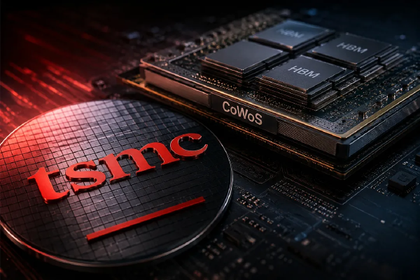
GlobalFoundries (GF) has signed a multiyear manufacturing agreement with Taiwan Semiconductor Manufacturing Company (TSMC) valued at approximately $2 billion, establishing a US-based supply of silicon interposers for TSMC’s Chip-on-Wafer-on-Substrate (CoWoS) advanced packaging ecosystem.
Announced on October 8, 2026, the agreement will expand manufacturing capacity at GF’s facility in Malta, New York. Volume production is expected to begin ramping in the first half of 2028, with the initial agreement spanning five years and providing a framework for future capacity expansion as demand grows. The companies’ announcement is available in the official GlobalFoundries release.
The deal targets a critical component in modern AI accelerators: the silicon interposer, which enables high-density communication between compute dies and high-bandwidth memory (HBM). GF also identifies embedded deep trench capacitors (eDTCs) among the advanced packaging technologies supported by the manufacturing expansion.
For TSMC, the agreement adds a US-based source for an essential component of its advanced packaging supply chain. For GF, it expands the company’s role beyond conventional wafer fabrication into the specialized manufacturing infrastructure supporting increasingly complex AI and high-performance computing systems.
The agreement does not, by itself, establish a complete US-based CoWoS packaging operation. Silicon-interposer manufacturing is one stage in a larger process that also depends on logic and memory supply, substrates, assembly, testing, equipment availability, and production yield.
🧩 CoWoS Technology and the Role of Silicon Interposers #
CoWoS is TSMC’s 2.5D advanced packaging technology for integrating multiple semiconductor dies into a single package. It is particularly important for AI accelerators, which combine high-performance compute dies with multiple HBM stacks to meet demanding bandwidth and throughput requirements.
Rather than connecting every component through conventional package-substrate wiring, CoWoS places dies on an interposer or a related high-density interconnect structure. This creates a denser communication fabric within the package and helps reduce the physical distance between compute and memory components.
How silicon interposers connect compute and memory #
A silicon interposer is a thin silicon structure containing high-density wiring and, in conventional silicon-interposer implementations, through-silicon vias (TSVs). These vertical connections allow signals to travel through the interposer between the dies above and the package substrate below.
The interposer provides a dense routing layer for communication among compute dies, memory stacks, and other integrated components. Its electrical characteristics and routing density are particularly important when a package must sustain high bandwidth across numerous connections.
For AI accelerators, the resulting architecture addresses a central system-design challenge: processors must move large volumes of data between compute units and memory without excessive latency or energy consumption.
As models and accelerator configurations grow, package design becomes increasingly constrained by interconnect density, memory bandwidth, power delivery, signal integrity, thermal management, and manufacturing yield.
Why silicon interposers matter for AI accelerators #
Modern AI performance depends on more than the number of arithmetic units or the transistor density of an individual die. The ability to supply those units with data efficiently can become a system-level bottleneck.
HBM provides high memory bandwidth, but realizing its full benefit requires dense, reliable connections between memory stacks and the compute dies they serve. Silicon interposers help provide these connections within a compact package.
Their advantages include:
- High interconnect density: Fine-pitch routing supports a large number of connections between compute and memory dies.
- Bandwidth and latency: Short, densely routed on-package connections facilitate high-throughput communication.
- Power efficiency: Efficient data movement can reduce the energy required to transfer information between dies.
- Heterogeneous integration: Multiple dies can be combined into a larger system without requiring every function to be fabricated on one monolithic processor.
These benefits are relevant to high-performance products developed by companies such as NVIDIA and AMD. However, larger packages introduce additional manufacturing challenges. As interposer area increases, defect sensitivity, routing complexity, thermal behavior, and yield become increasingly important.
The three main CoWoS implementations #
TSMC’s CoWoS family encompasses three principal approaches: CoWoS-S, CoWoS-R, and CoWoS-L. They differ in their interconnect structures and the trade-offs they make among routing density, scalability, manufacturability, and cost.
CoWoS-S: Silicon interposer #
CoWoS-S uses a silicon interposer with TSVs to provide dense connections between logic dies and HBM stacks. Its fine-pitch routing makes it suitable for demanding high-performance computing and AI packages.
The principal challenge is the manufacturing complexity associated with large silicon interposers. As package dimensions increase, maintaining acceptable defect density and yield becomes more difficult. Larger structures can also increase material requirements and manufacturing costs.
The silicon interposers covered by GF’s agreement are intended to support TSMC’s advanced packaging ecosystem, particularly its silicon-interposer supply chain.
CoWoS-R: Redistribution-layer interposer #
CoWoS-R uses a redistribution-layer (RDL) structure incorporating polymer-based dielectric materials and copper wiring. Instead of relying on a full silicon interposer across the entire package, it uses a different interconnect architecture to balance routing requirements and manufacturing considerations.
Its suitability depends on package dimensions, electrical requirements, routing density, and the characteristics of the dies being integrated.
CoWoS-L: Hybrid interconnection #
CoWoS-L combines large-area RDL routing with localized silicon interconnect (LSI) structures. The RDL provides broader package-level connectivity, while localized silicon elements deliver dense interconnections in areas that require them.
This hybrid approach offers an alternative to using one large silicon interposer for every interconnect function. Its objective is to balance high-density communication requirements with package-scale integration and manufacturing constraints.
The distinctions among these architectures are explored further in KAD’s analysis of Samsung iCube versus TSMC CoWoS advanced packaging.
📈 TSMC’s CoWoS Capacity Expansion and Technology Roadmap #
Advanced packaging has become a significant constraint on AI accelerator production. Increasing front-end wafer output does not necessarily increase the number of completed accelerators if interposer fabrication, packaging, or testing capacity cannot keep pace.
TSMC’s response involves expanding manufacturing capacity while developing packaging architectures capable of supporting larger compute dies, additional HBM stacks, and more complex multi-die configurations.
CoWoS capacity expansion estimates #
Industry estimates cited in the supplied report indicate substantial growth in TSMC’s monthly CoWoS capacity over the second half of the decade.
| Period | Reported or projected monthly capacity |
|---|---|
| End of 2024 | Approximately 35,000 wafers |
| End of 2026 | Approximately 130,000–140,000 wafers |
| End of 2028 | Approximately 260,000 wafers |
These figures represent reported estimates and projections rather than guaranteed production output or confirmed commitments. Actual capacity will depend on equipment installation, process qualification, yield, customer demand, and the availability of supporting materials and components.
The figures should also be interpreted within the broader manufacturing flow. Additional CoWoS capacity does not automatically translate into equivalent finished-accelerator output because logic dies, HBM, substrates, assembly, and testing must all be available in sufficient quantities.
GF’s agreement addresses one part of this equation by expanding the supply of silicon interposers. Its contribution to overall packaging throughput will depend on qualification, production scale, and integration with TSMC’s manufacturing operations.
Larger interposers and increasing HBM integration #
TSMC’s advanced packaging roadmap also reflects the need to accommodate increasingly large compute and memory configurations within individual packages.
According to the reported roadmap described in the supplied material, interposer implementations spanning approximately 5.5 times the reticle field size entered mass production in 2026. A larger configuration spanning approximately 14 times the reticle field size is planned for 2028, with support for up to 20 HBM stacks. Configurations with up to 24 HBM stacks are anticipated in the 2029 timeframe.
These figures should be treated as reported roadmap targets rather than guaranteed specifications for every product or package generation.
Scaling interposers creates several engineering challenges. Larger silicon structures increase the impact of defects on overall yield, while denser routing increases design and process complexity. Additional HBM stacks introduce further requirements for power delivery, thermal management, signal integrity, mechanical stability, and testing.
These constraints explain why advanced packaging requires simultaneous progress in materials, process integration, inspection, and manufacturing control—not simply more production lines.
As package complexity increases, a reliable silicon-interposer supply becomes a more important element of the broader AI semiconductor manufacturing strategy.
🏭 GlobalFoundries’ Advanced Packaging Capabilities #
GlobalFoundries is a semiconductor foundry headquartered in Malta, New York. Established in 2009, the company originated as a joint venture involving Mubadala and AMD and has since developed a manufacturing portfolio focused on differentiated process technologies and specialty semiconductor applications.
Its operations span the United States, Europe, and Asia, with manufacturing facilities supporting markets such as communications, automotive, industrial systems, power management, and cloud infrastructure.
Rather than competing exclusively on the smallest logic process nodes, GF emphasizes specialized manufacturing capabilities and integration technologies. Its agreement with TSMC builds on investments in silicon interposers, silicon photonics, and wafer bonding.
The 65PKG silicon-interposer platform #
GF’s 65PKG silicon-interposer platform received mass-production certification in 2024 and was reported to have achieved Technology Readiness Level 9 (TRL 9).
The platform incorporates TSV technology and supports wafer-to-wafer and chip-to-wafer integration. These capabilities provide a foundation for connecting different semiconductor components within advanced packaging architectures.
Heterogeneous integration is increasingly important because system-level performance improvements often come from combining specialized compute, memory, and supporting dies rather than fabricating every function on a single large die.
A mature interposer platform can reduce the technology-development burden associated with introducing a new manufacturing program. However, technology readiness is not equivalent to immediate high-volume production for a new customer. TSMC-specific qualification, process integration, yield optimization, reliability testing, and manufacturing execution will remain essential.
SCALE co-packaged optics #
In May 2026, GF introduced its SCALE co-packaged optics (CPO) solution for AI data center applications. The company reported demonstrations involving 8λ and 16λ bidirectional dense wavelength-division multiplexing (DWDM) transmission.
CPO seeks to bring optical connectivity closer to processors and switching hardware, addressing limitations associated with moving large volumes of data over conventional electrical interconnects.
As AI clusters expand, bandwidth density, power consumption, signal integrity, and the reach of electrical links become increasingly important design constraints. Silicon photonics and optical integration offer potential ways to improve data movement across large-scale computing infrastructure.
Although CPO and silicon interposers solve different integration problems, both illustrate the growing importance of advanced manufacturing technologies in scaling AI systems.
SLATE wafer-to-wafer bonding #
In June 2026, GF announced that its SLATE wafer-to-wafer bonding technology was production-ready on its 9SW radio-frequency (RF) platform.
Wafer-to-wafer bonding supports the integration of semiconductor structures through precisely controlled bonding interfaces. Successful manufacturing depends on factors such as alignment accuracy, bond quality, defect control, thermal compatibility, and process yield.
GF’s development of bonding, photonics, and silicon-interposer technologies demonstrates a broader approach to semiconductor integration. These capabilities can serve different markets, but they share a common requirement: combining specialized structures reliably within increasingly complex semiconductor systems.
GF’s strategic position in the US supply chain #
The TSMC agreement gives GF an opportunity to extend its manufacturing footprint into a critical part of the AI accelerator supply chain.
GF senior vice president Ed Kaste has emphasized the increasing importance of advanced packaging to the performance, power efficiency, and scalability of next-generation AI systems. The agreement applies that manufacturing strategy to a component that has traditionally depended heavily on Asian semiconductor production capacity.
For TSMC, a qualified US-based source could diversify its supply of silicon interposers. For GF, the partnership creates a stronger connection to the advanced AI and high-performance computing markets without requiring it to manufacture the leading-edge compute dies themselves.
The commercial outcome will depend on the company’s ability to meet TSMC’s technical requirements, achieve competitive yields, and scale production while maintaining consistent quality.
🔍 What the $2 Billion Agreement Means for the Semiconductor Industry #
The GF–TSMC agreement reflects a broader shift in the semiconductor industry. Competition for AI infrastructure is no longer determined by front-end wafer fabrication alone. Advanced packaging, HBM integration, interconnect technology, and specialized manufacturing components increasingly influence the performance and availability of complete computing systems.
Diversifying the advanced packaging supply chain #
The addition of a US-based silicon-interposer source could improve geographic diversification within TSMC’s CoWoS supply chain.
Regional manufacturing does not eliminate supply-chain risk. Semiconductor production remains dependent on globally distributed equipment, materials, process expertise, logistics, and downstream facilities. Nevertheless, adding qualified production capacity can reduce reliance on a limited number of suppliers or manufacturing locations.
The agreement also illustrates how investment in US semiconductor manufacturing is extending beyond front-end fabrication into specialized components and advanced integration technologies.
The distinction is important: manufacturing an interposer in the United States does not necessarily mean that every subsequent packaging, assembly, and testing step will occur domestically. The degree of supply-chain localization will depend on the capabilities and locations of the facilities participating in the complete production flow.
Addressing AI chip manufacturing bottlenecks #
The expansion of silicon-interposer capacity could alleviate one constraint affecting AI accelerator production, especially as packages incorporate more compute dies and memory stacks.
However, the overall supply chain remains dependent on several interconnected inputs:
- Front-end wafer fabrication: Sufficient logic dies must be available from qualified manufacturing processes.
- HBM supply: Memory production and integration must keep pace with accelerator demand.
- Interposer fabrication: High-density interconnect structures must meet the required dimensions, electrical characteristics, and quality standards.
- Substrates and materials: Package substrates and other specialized materials must be available in sufficient volumes.
- Assembly and testing: Packaging lines, equipment, and test infrastructure must support the required throughput and reliability.
Increasing capacity in one stage does not guarantee a proportional increase in completed accelerator shipments. If another input becomes constrained, total production may remain limited.
Because GF’s production ramp is planned for the first half of 2028, the agreement represents a medium-term capacity investment rather than an immediate increase in available CoWoS output.
Expanding GlobalFoundries’ role in AI infrastructure #
For GF, the agreement creates an opportunity to deepen its participation in the AI semiconductor market through differentiated manufacturing technologies.
Its silicon-interposer platform addresses high-density chip integration, while silicon photonics and wafer bonding support other approaches to managing connectivity and system complexity.
The TSMC partnership may also strengthen GF’s position as semiconductor designers and manufacturers seek qualified suppliers for specialized packaging components. However, technological capability alone does not guarantee commercial success.
Long-term value will depend on production yield, cost competitiveness, capacity utilization, customer qualification, and the ability to manufacture reliably at scale.
The partnership also reinforces an important competitive dynamic: advanced packaging is becoming a strategic differentiator alongside logic process technology. TSMC’s position in this market is discussed in KAD’s analysis of advanced AI chip packaging and the competition with Intel.
Commercial implications and remaining uncertainties #
Although the agreement is valued at approximately $2 billion, the public announcement does not provide a detailed breakdown of production volumes, pricing, or capacity commitments.
The headline value should therefore be understood as the reported value of a multiyear manufacturing agreement, not as a disclosed annual revenue run rate or a guarantee of any particular level of output.
The initial five-year term and provision for future expansion establish a commercial framework for scaling production as customer requirements evolve. Actual results will depend on qualification milestones, demand, operating costs, and manufacturing performance.
For both companies, execution will be as important as the strategic rationale. GF must establish production that meets TSMC’s requirements, while TSMC must integrate the additional interposer supply with its own packaging processes and other essential inputs.
✅ Conclusion: A New US Source for Silicon Interposers #
GlobalFoundries’ approximately $2 billion agreement with TSMC represents a significant development in the US advanced semiconductor packaging supply chain. By expanding silicon-interposer manufacturing at its Malta, New York, facility, GF is expected to establish a US-based source of components for TSMC’s CoWoS ecosystem, with production ramp-up planned for the first half of 2028.
The agreement highlights the growing importance of silicon interposers and heterogeneous integration in AI accelerators, where memory bandwidth, interconnect density, power efficiency, and manufacturing yield increasingly shape system-level performance.
It also illustrates the limits of semiconductor supply-chain diversification. Domestic interposer manufacturing can reduce dependence on overseas sources for a critical component, but the complete production process still relies on HBM, substrates, equipment, assembly, testing, and other globally distributed capabilities.
The partnership’s impact will ultimately depend on production ramp-up, technical qualification, yield, and the availability of complementary manufacturing inputs. If GF successfully scales its operations, the agreement could improve geographic resilience and add capacity to an important part of the AI accelerator supply chain.
As compute dies grow larger and HBM integration becomes more complex, the ability to manufacture advanced packaging components reliably and at high volume will remain a major factor in determining how quickly the semiconductor industry can meet demand for AI and high-performance computing.