Nikon Challenges ASML with Aggressive ArF Lithography Pricing
For years, ASML has dominated the global lithography market. While the Dutch company holds an uncontested monopoly in Extreme Ultraviolet (EUV) lithography, it has also steadily strengthened its position in Deep Ultraviolet (DUV) systems, pushing former industry leaders such as Nikon and Canon into increasingly smaller market niches.
However, Nikon is no longer content to remain on the sidelines.
The Japanese optical technology giant has signaled a renewed push into the semiconductor equipment market by aggressively targeting new ArF lithography orders with lower pricing than ASML. The move marks one of the clearest attempts in years to challenge ASML’s dominance and re-establish Nikon as a serious competitor in advanced DUV lithography.
🔬 ASML’s Dominance in Modern Lithography #
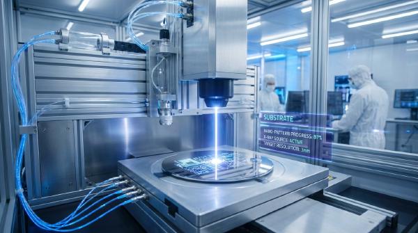
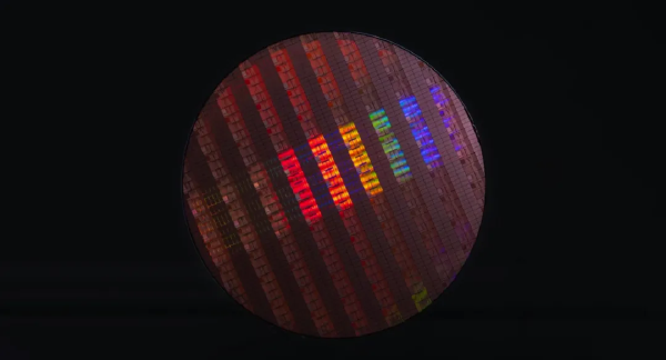
The semiconductor industry’s most advanced chips depend heavily on lithography systems, which project intricate circuit patterns onto silicon wafers.
Today, ASML occupies an extraordinarily powerful position:
- It is the sole supplier of EUV lithography systems.
- It controls the majority of the advanced DUV lithography market.
- Leading foundries and integrated device manufacturers rely on its equipment for cutting-edge process nodes.
ASML’s EUV systems are indispensable for manufacturing advanced logic chips at the most sophisticated process technologies. At the same time, its DUV product family remains deeply embedded throughout semiconductor production lines worldwide.
This dual-market leadership has allowed ASML to become one of the most strategically important companies in the global semiconductor supply chain.
💰 Nikon’s New Strategy: Compete on Price #
According to recent comments from Nikon CEO Yasuhiro Ohmura, the company is actively pursuing new ArF lithography orders by offering pricing below that of comparable ASML systems.
Nikon believes it possesses a significant cost advantage due to its vertically integrated manufacturing approach.
Unlike many competitors, Nikon produces a substantial portion of its key components internally, allowing the company to:
- Reduce supply chain costs
- Improve manufacturing efficiency
- Maintain tighter control over production
- Offer more competitive pricing
Reports indicate that Nikon is currently negotiating with major semiconductor manufacturers across Asia and the Americas, with several potential orders reportedly approaching finalization.
For semiconductor manufacturers facing rising capital expenditure requirements, lower equipment costs can be highly attractive.
⚙️ Why ArF Lithography Still Matters #
While EUV technology receives most of the industry’s attention, ArF lithography remains one of the most important workhorses in semiconductor manufacturing.
Understanding ArF Technology #
ArF lithography utilizes an argon fluoride excimer laser operating at a wavelength of 193 nanometers.
It represents the most advanced category of DUV lithography and is generally divided into two major classes:
- ArF Dry
- ArF Immersion
Immersion systems offer superior resolution and have become the standard for advanced manufacturing.
Many of ASML’s flagship DUV products, including the Twinscan NXT series, fall into this category.
Supporting Advanced Process Nodes #
Despite the rise of EUV, ArF lithography remains essential because:
- Not every chip layer requires EUV exposure.
- Multi-patterning techniques enable ArF systems to support advanced process nodes.
- Manufacturing costs can be significantly reduced by limiting EUV usage.
With sophisticated multi-patterning approaches, ArF immersion lithography can contribute to the production of chips down to the 7nm generation and beyond.
As a result, even the world’s most advanced semiconductor fabs continue to rely heavily on DUV systems.
📈 Why Semiconductor Manufacturers Still Need DUV #
A common misconception is that EUV has completely replaced DUV.
In reality, semiconductor production relies on a mix of lithography technologies.
Cost Considerations #
EUV systems are among the most expensive manufacturing tools ever built.
Using EUV for every mask layer would dramatically increase production costs.
Foundries therefore carefully optimize process flows by combining:
- EUV for critical layers
- ArF immersion lithography for less demanding layers
This hybrid approach improves economics while maintaining competitive yields.
Installed Infrastructure #
Many fabs have already invested billions of dollars in DUV infrastructure.
Replacing all existing equipment is neither practical nor economically desirable.
As a result, advanced DUV systems continue to generate strong demand, especially among:
- Mature-node manufacturers
- Specialty chip producers
- Memory manufacturers
- Cost-sensitive foundries
This creates an opportunity for competitors like Nikon to regain market share.
📷 From Camera Giant to Lithography Pioneer #
Most consumers recognize Nikon and Canon for their cameras and optical products.
Within the semiconductor industry, however, both companies once played a far larger role.
Japan’s Historic Leadership #
During the 1980s and 1990s, Japanese firms dominated much of the global lithography market.
At the time:
- Nikon was a leading supplier of semiconductor manufacturing equipment.
- Canon maintained a significant presence in lithography systems.
- ASML was still a relatively small competitor.
Nikon’s reputation was built largely on its exceptional optical engineering capabilities, an area where the company remains highly respected today.
Intel’s Former Dependence on Nikon #
At its peak, Intel sourced a substantial portion of its lithography equipment from Nikon.
In some periods, Nikon reportedly supplied the majority of Intel’s lithography systems.
However, the industry’s transition toward EUV technology reshaped competitive dynamics dramatically.
ASML invested heavily and early in EUV development, ultimately securing exclusive leadership in the technology. This strategic advantage helped propel ASML to its current dominant position.
🎯 Nikon’s Remaining Competitive Advantages #
Although Nikon no longer competes in EUV lithography, the company continues to possess strengths that resonate with semiconductor manufacturers.
Optical Expertise #
Nikon’s decades of experience in precision optics remain a valuable differentiator.
The company is particularly recognized for:
- Lens design
- Optical accuracy
- Precision alignment systems
- Imaging consistency
These strengths directly influence lithography performance.
Critical Dimension Uniformity #
One area where Nikon systems have historically performed well is Critical Dimension (CD) uniformity.
CD uniformity measures how consistently features are printed across an entire wafer.
Strong performance in this area contributes to:
- Improved yields
- Better process control
- Enhanced manufacturing consistency
For many fabs, these metrics remain critical purchasing considerations.
Lower Capital Expenditure #
Perhaps Nikon’s strongest weapon is cost.
Industry observers estimate that Nikon’s pricing strategy may offer discounts ranging from 20% to 30% compared with equivalent ASML systems.
For semiconductor manufacturers building or expanding fabrication capacity, such savings can translate into:
- Lower upfront investment
- Faster return on capital
- Greater equipment purchasing flexibility
In an industry where a modern fab can cost tens of billions of dollars, even modest equipment savings become highly significant.
🏭 What This Means for the Semiconductor Industry #
Nikon’s strategy is unlikely to threaten ASML’s EUV monopoly in the near term.
However, the DUV market represents a different competitive landscape.
Several factors could work in Nikon’s favor:
Continued Demand for Mature Nodes #
Automotive, industrial, and IoT chips continue to rely heavily on mature process technologies where DUV remains dominant.
Rising Cost Pressures #
Chipmakers are increasingly focused on controlling capital expenditures as fabrication costs continue to rise.
Diversified Supply Chains #
Many manufacturers seek to reduce dependence on a single equipment supplier whenever practical.
A credible alternative supplier can improve purchasing leverage and operational flexibility.
🔮 Outlook: Can Nikon Regain Market Share? #
Nikon’s latest move signals that competition in the lithography market is far from over.
While ASML remains the undisputed leader in advanced lithography technology, the enormous installed base of DUV manufacturing creates room for alternative suppliers to compete.
By leveraging:
- Competitive pricing
- Strong optical engineering
- Proven ArF technology
- Lower total acquisition costs
Nikon aims to position itself as a compelling complementary solution rather than a direct replacement for ASML.
Whether the strategy succeeds will depend on how aggressively semiconductor manufacturers pursue cost optimization over the next several years.
One thing is certain: as semiconductor demand continues to grow and fabrication costs rise, every percentage point of efficiency matters. In that environment, Nikon’s willingness to challenge the market leader through pricing and technical differentiation could make it one of the industry’s most closely watched comeback stories.