AMD EPYC Venice: 256 Zen 6 Cores, 2nm Process and 73,000 AI Agents per Rack
An in-depth look at the architecture and technology behind AMD’s 6th Gen EPYC server processors.
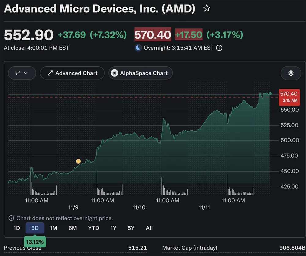
AMD has been making significant moves in the data center market. Its latest financial results showed that third-quarter data center revenue nearly doubled, while its stock price climbed more than 13% over three trading days.
AMD has now officially launched its 6th Gen EPYC 9006 SP7 server processors, codenamed “Venice.” The new CPUs use the SP7 platform, and the first AMD Helion Agentic AI rack systems are scheduled to begin shipping this month.
During AMD’s third-quarter earnings call, Chair and CEO Dr. Lisa Su said early demand for Venice was stronger than for any previous EPYC generation. AMD began shipping the processors in Q3, and OEM and ODM partners have already committed to more than 240 platform designs. That’s a 20% increase over the 5th Gen EPYC “Turin” launch. Cloud instances are expected to become available progressively in early 2027.
The early adoption figures suggest that Venice is gaining traction with server manufacturers. But what makes this generation attractive to data center operators?
At a technical briefing in Las Vegas, AMD executives and engineers discussed the design decisions behind the 6th Gen EPYC family. The presentation covered everything from the changing CPU requirements of agentic AI to the reasons for offering several processor configurations. It also examined the Venice SoC, Zen 6 and Zen 6c cores, memory architecture, I/O, power management, and new ways to reduce the cost of server memory.
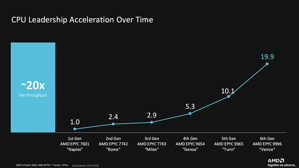
Since the first-generation EPYC “Naples” arrived in 2018, AMD has introduced six generations of server processors. The company says overall performance has increased by nearly 20 times over that period.
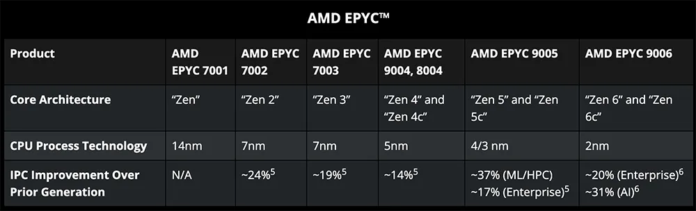
The flagship Venice configuration offers up to 256 cores and 512 threads, memory bandwidth of up to 1.6 TB/s, and operating frequencies reaching 5.3 GHz. Its compute dies are manufactured using a 2nm process.
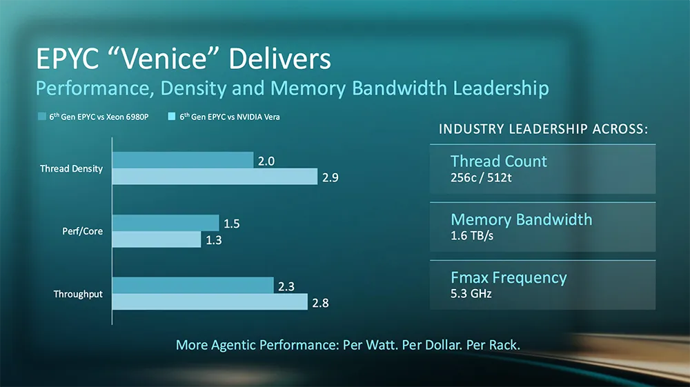
AMD’s comparisons with Intel Xeon 6980P and NVIDIA Vera highlight improvements in thread density, per-core performance, and overall throughput. The company’s central argument is that Venice can deliver better performance per watt, per dollar, and per rack for agentic AI infrastructure.
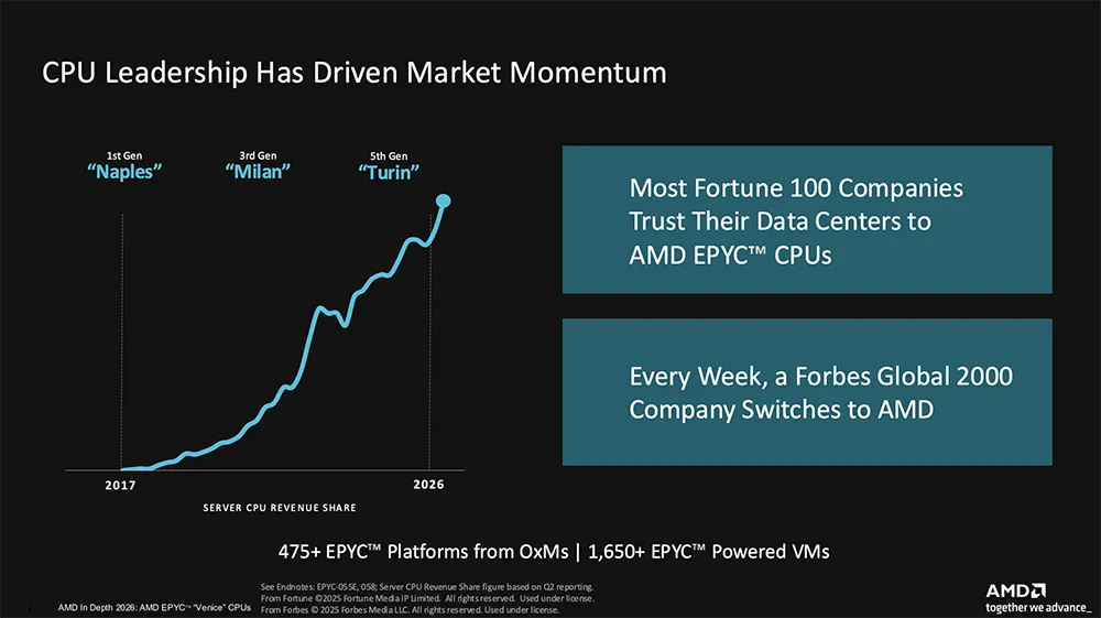
AMD also provided an update on its position in the server CPU market. According to the company’s presentation, its market share moved from the low-40% range at the beginning of the year to the mid-40% range. AMD also said that most US Fortune 100 companies now use EPYC processors in their data centers.
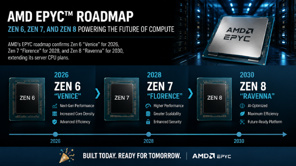
The company’s roadmap extends beyond Venice. The 7th Gen EPYC “Florence” is planned for 2028, with two core architectures, next-generation process technology and memory, and the introduction of AI Compute Extensions (ACE). AMD has also started development of its 8th Gen EPYC “Ravenna.”
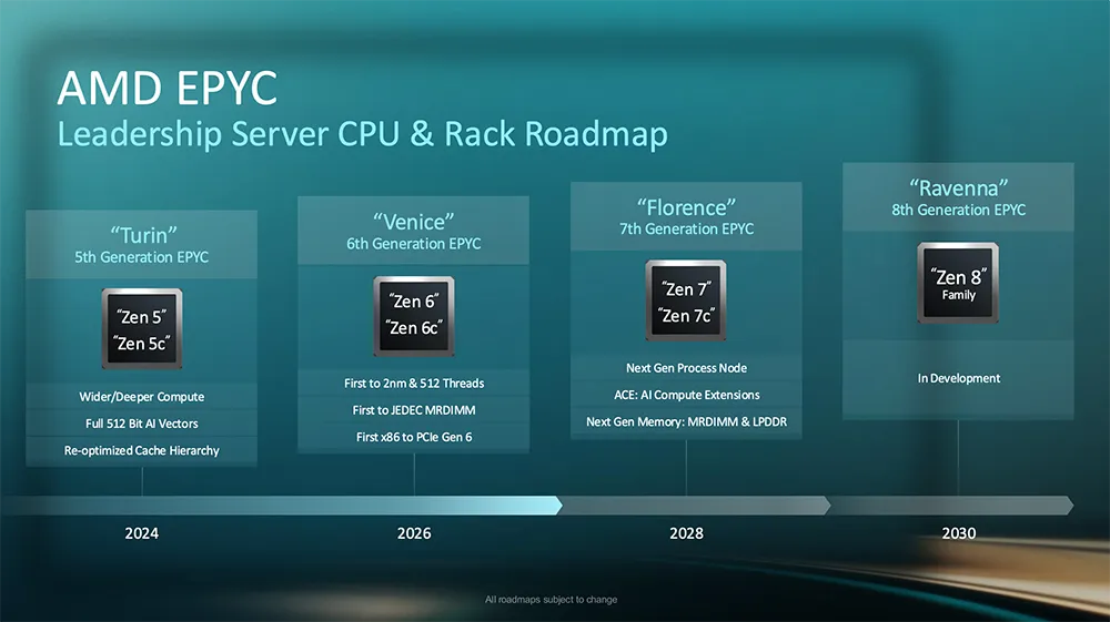
Agentic AI is increasing demand for CPU resources throughout the data center. Model execution still depends heavily on GPUs, but agents also need CPUs for orchestration, retrieval, tool execution, code compilation, and isolated environments. This creates an opportunity for AMD to expand EPYC’s role in next-generation AI infrastructure.
This article examines the technical details and product highlights of the 6th Gen EPYC family, including:
- The four 6th Gen AMD EPYC product configurations
- Performance across agentic AI, cloud, HPC, and enterprise workloads
- AMD Helion Agentic AI racks and software tools
- The Venice SoC, CCDs, I/O dies, and internal data paths
- Zen 6c microarchitecture improvements
- New Zen 6 instructions and AI computing enhancements
- DDR5, LPDDR5X, and CXL 3.1 memory support
- MEXT memory tiering and DRAM cost reduction
- PCIe 6.0 and the SDXI data movement engine
- Power management technologies
- RAS, confidential computing, and platform security
01. Four EPYC Products: Up to 256 Cores and 5.3 GHz #
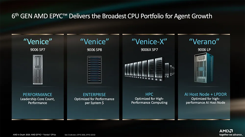
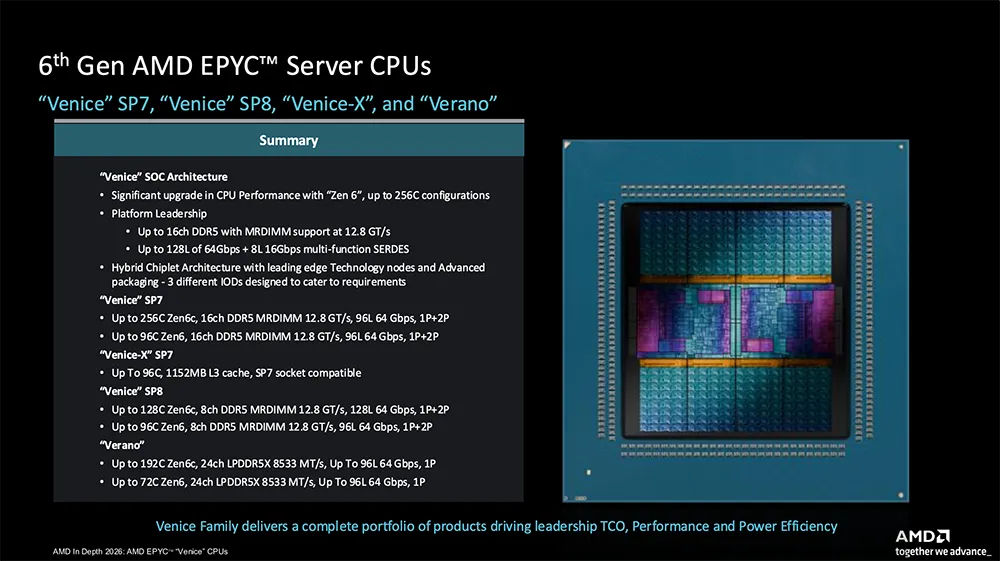
The 6th Gen AMD EPYC portfolio is not a single processor design aimed at every type of server. It consists of four product configurations: Venice SP7, Venice SP8, Venice-X, and Verano. Each targets a different balance of compute density, frequency, memory, and I/O.
-
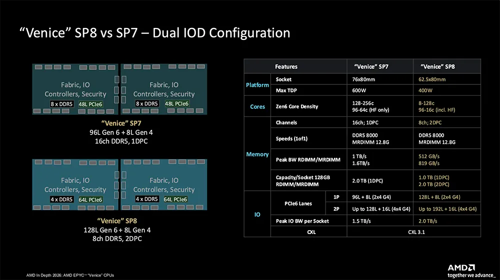
(1) Venice 9006 SP7: The flagship configuration targets workloads that need high compute throughput. Its compact socket measures 76 × 80 mm. The high-density Zen 6c version supports up to 256 cores and 512 threads, with frequencies reaching 4.1 GHz. The high-frequency Zen 6 version supports up to 96 cores and 192 threads, reaching 5.3 GHz. SP7 supports both single-socket and dual-socket systems. A single socket provides up to 96 PCIe Gen 6 lanes, with twice the bandwidth per lane compared with the previous generation. Memory support includes JEDEC-compliant MRDIMM-12800, delivering up to 1.6 TB/s per socket. Configurable TDP ranges from 400W to 600W. These processors have begun shipping.
-
(2) Venice 9006 SP8: SP8 is designed for enterprise systems that need substantial I/O capacity without the same compute requirements as the flagship platform. Its package measures 62.5 × 80 mm and uses a new I/O die. The platform supports up to 128 Zen 6c cores or 96 Zen 6 cores, eight memory channels with two DIMMs per channel, and up to 128 PCIe Gen 6 lanes per socket. Its launch is planned for the first half of 2027.
-
(3) Venice-X 9006X SP7: This version targets HPC applications that benefit from a large last-level cache. It combines Zen 6 with 3D V-Cache, using stacked cache to reduce the need for slower memory accesses. The configuration offers up to 96 cores and as much as 1,152 MB of total L3 cache. AMD plans to release it in the second half of 2027.
-
(4) Verano 9006 LP: Verano is designed for AI host nodes where memory power consumption matters. It uses a 24-channel LPDDR5X interface and interchangeable SOCAMM modules. Moving more of the memory subsystem toward low-power LPDDR5X is intended to reduce power consumption outside the CPU cores. Its launch is also scheduled for the second half of 2027.
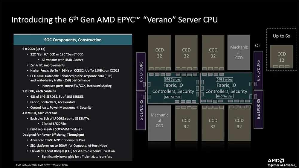
Verano uses a BGA package, whereas Venice SP7 uses an SMLGA socket. Despite that packaging difference, the two platforms reuse the logical data paths connecting the CCDs and I/O dies. AMD says Verano therefore retains the same core-level performance capabilities as SP7.
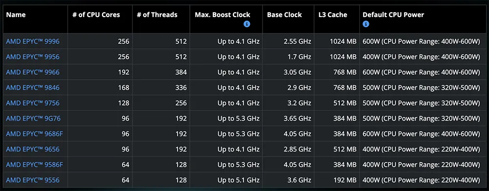
The model numbering for Venice 9006 SP7 processors follows the naming convention shown below. Models carrying the “F” suffix are high-frequency versions based on Zen 6 cores.
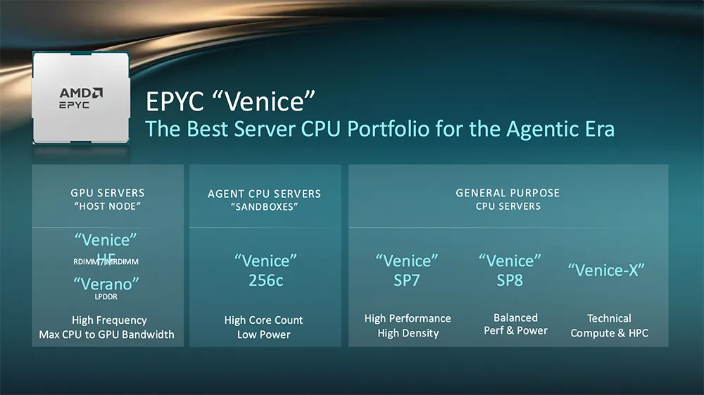
The four configurations reflect the fact that server workloads do not all benefit from the same operating point. Some prioritize peak single-thread performance, while others need as many cores as possible within a fixed power envelope.
The chart below compares performance against power consumption. Its utilization range of 15% to 100% represents the proportion of CPU cores active simultaneously across the SoC.
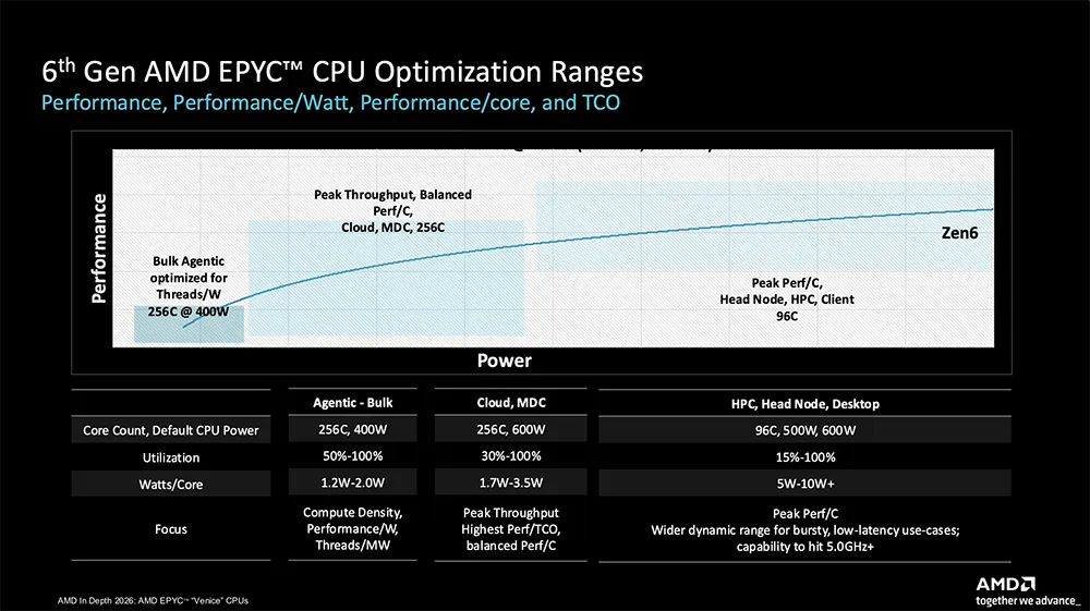
HPC and host-node workloads often depend on strong single-core performance. They can also be bursty and sensitive to latency. These applications benefit from a wide dynamic operating range, which is why AMD pushes the maximum frequency of its Zen 6 cores to 5.3 GHz.
Cloud and agentic-bulk workloads have a different profile. When only some CPU cores are busy, the power budget can be concentrated on those active cores. The processor needs enough frequency and power headroom to turn that additional budget into useful performance. AMD’s Zen 6c cores therefore support frequencies of up to 4.1 GHz.
When the overall SoC power limit is reduced to 400W, compute density becomes a more important design target. In this range, AMD places greater emphasis on threads per megawatt and performance per watt.
02. EPYC Venice for Agentic AI, Cloud, HPC, and Enterprise Workloads #
AMD describes the EPYC 9006 SP7 as “the best CPU for the agentic AI era.” The processor family is intended to cover three major CPU roles in agentic AI infrastructure: general-purpose services, AI host nodes, and agent sandboxes.
AMD’s performance presentation highlights several workload categories:
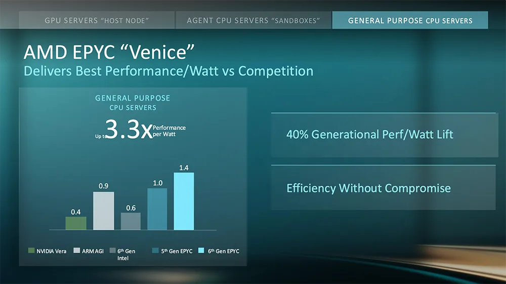
- (1) General-purpose computing: AMD reports up to 40% better performance per watt than the previous generation. Across its selected comparisons, Venice delivers approximately 1.5 to 3.5 times the performance of processors including NVIDIA Vera, Arm AGI, and 6th Gen Intel Xeon.
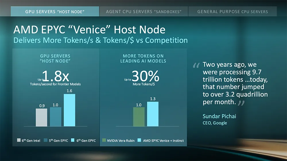
- (2) High-frequency host nodes: Configurations running at up to 5.3 GHz are designed for CPU-intensive host tasks. AMD reports up to 1.6 times the LLM output throughput of the previous generation and 1.8 times that of 6th Gen Xeon.
- (3) High-density agent servers: For agent sandbox workloads, AMD says its high-density EPYC processors deliver around 3.3 times as many agents per CPU watt as NVIDIA Vera and approximately 2.5 times as many as Intel Xeon 6980P.
AMD also tested agent capacity under a matched 35kW rack power envelope. Systems based on the EPYC 9996 support approximately 1.18 times as many agents as systems using default power-management settings.
The company’s argument for Venice rests on several related metrics: token output per dollar, agent capacity, agent capacity per watt, and overall operating efficiency. These measures are particularly relevant to agentic workloads, where a system may run many independent tasks rather than concentrate all its resources on a single model invocation.
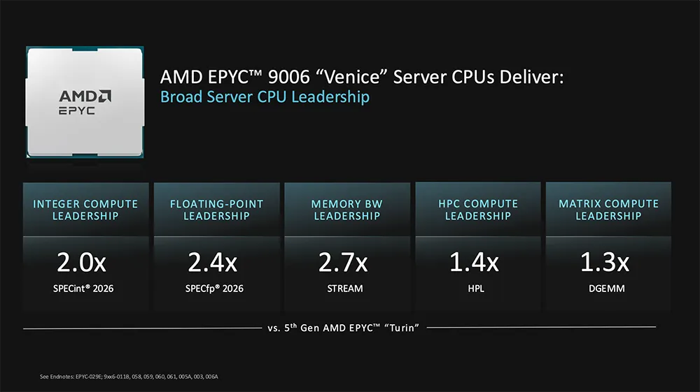
Across integer computing, floating-point workloads, memory bandwidth, HPC, and matrix operations, AMD reports performance improvements of approximately 1.3 to 2.7 times over the previous generation.
An agentic AI system does more than execute model inference. CPU resources are also needed for model invocation, retrieval, request routing, document parsing, code compilation, and sandbox execution. As the number of concurrent agents grows, these supporting tasks can become a significant part of the infrastructure workload.
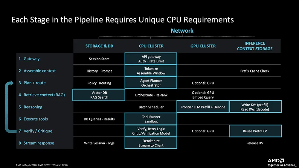
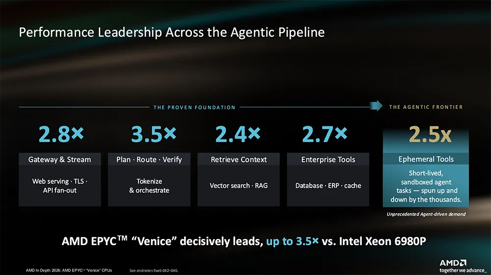
In AMD’s comparison of decoupled agent workflows with Intel Xeon 6980P, Venice delivers at least 2.4 to 2.8 times the performance in most tested scenarios. The advantage reaches 3.5 times in tokenization and orchestration workloads.
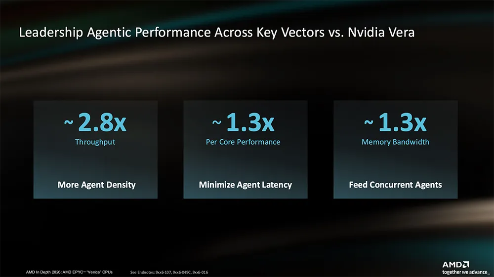
AMD also compared Venice with publicly available NVIDIA Vera results. Under the stated testing conditions, with each platform using its respective optimized compiler, AMD reports 2.8 times the throughput, 1.3 times the per-core performance, and 1.3 times the memory bandwidth.
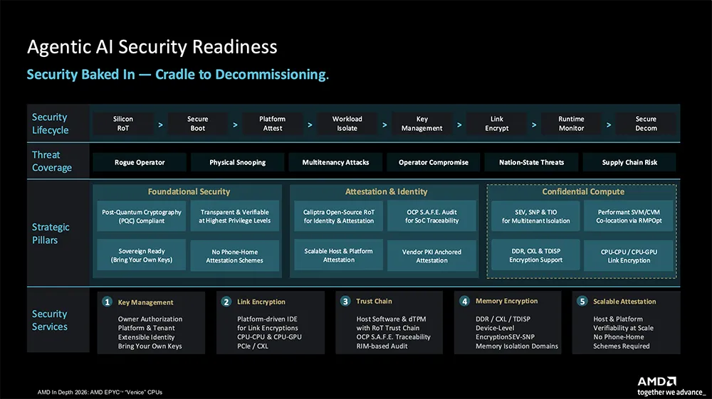
Security is another part of AMD’s agentic AI platform strategy. The company’s approach covers the full security lifecycle, including threat coverage, baseline hardware protections, remote attestation, identity verification, and confidential computing.
For enterprise and cloud workloads, AMD reports that systems based on the EPYC 9996 deliver up to 3.7 times the performance of systems using NVIDIA Vera CPUs. Against Intel Xeon 6980P, AMD reports up to 2.2 times the performance and twice the price-performance.
Microsoft Azure has announced a preview of Venice-based HDv2 instances, making it the first cloud provider to offer instances based on 6th Gen EPYC.
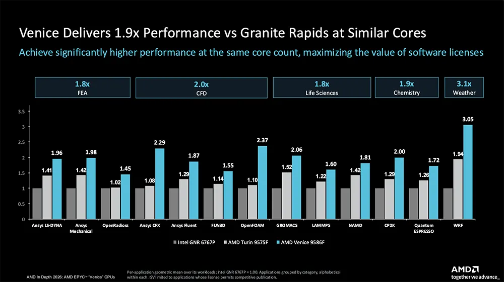
HPC is another important target. AMD points to published SPECrate results and the processor’s high memory bandwidth as advantages for demanding simulations in life sciences, quantum chemistry, and weather forecasting.
In single-node comparisons presented by AMD, Venice delivers 2.3 times the SPEC HPC 2021 performance and 2.2 times the STREAM benchmark performance of Intel Granite Rapids. The company also reports gains in finite element analysis, computational fluid dynamics, SPICE circuit simulation, and weather prediction.
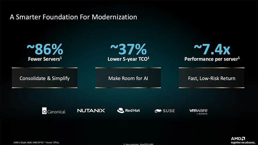
For enterprise customers, the value of a new server processor is measured by the applications it can consolidate and the operating costs it can reduce. AMD says that migrating from Intel Xeon Ice Lake systems to Venice can reduce the required server count by as much as 86% and lower five-year total cost of ownership by 37%.
Storage and database workloads also benefit from higher CPU throughput. AMD reports approximately 3.3 times the storage and database throughput of 6th Gen Xeon solutions.
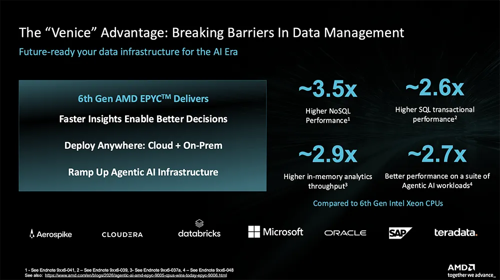
In Databricks testing cited by AMD, Venice delivers slightly more than 2.6 times the SQL transaction-processing performance, 3.5 times the NoSQL performance, and up to 2.7 times the performance across a group of agentic AI workloads compared with 6th Gen Intel Xeon.
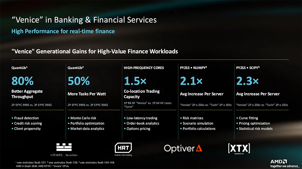
Financial and scientific software provide further examples. Compared with the previous generation, Venice increases total throughput in the open-source QuantLib financial library by around 80%, while improving completed tasks per unit of power by approximately 50%.
For NumPy and SciPy, AMD reports average single-server performance improvements of roughly 2.1 to 2.3 times.
The presentation also covers several industry-specific workloads:
- Manufacturing: Industrial software packages show performance improvements of approximately 1.3 to 1.6 times over the previous generation.
- Telecommunications: Venice processes around three times as much traffic per unit of power, potentially reducing operating costs for carriers.
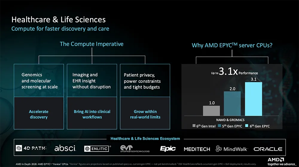
- Healthcare: Migrating from 6th Gen Intel Xeon platforms to Venice delivers up to three times the performance in molecular simulation workloads.
These figures are AMD’s reported results and depend on the systems, software, configurations, and test conditions used. They illustrate the company’s positioning of Venice as a platform for a broad range of CPU-intensive data center tasks, not just AI infrastructure.
03. Helion Agentic AI Racks: 36,864 Cores and More Than 73,000 Agents #
Venice is designed to provide the CPU resources needed by agentic AI systems. AMD’s Helion rack solutions combine those processors with rack-level infrastructure to deliver complete systems.
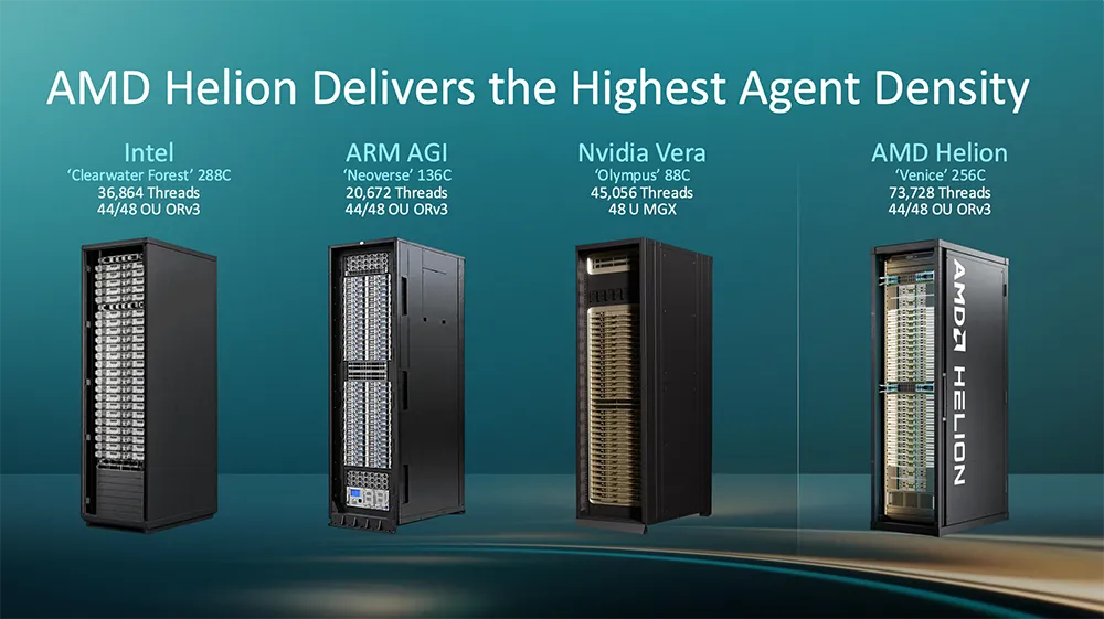
AMD’s presentation compares Helion with rack solutions built around Intel, Arm AGI, and NVIDIA Vera. The highest-density Helion configuration provides 73,728 threads.
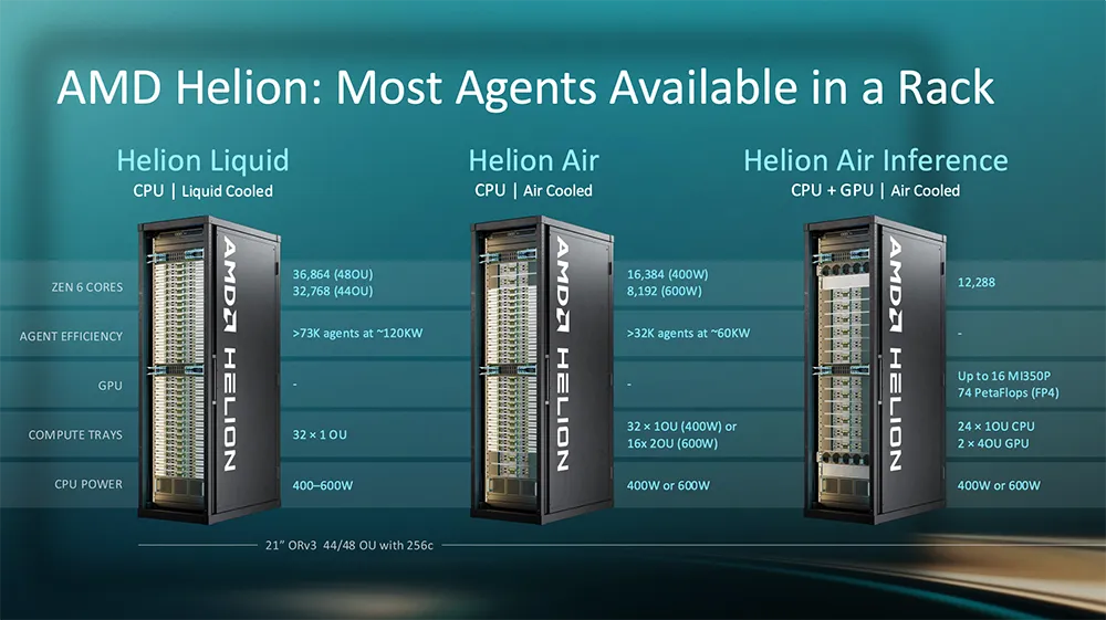
Helion comes in three deployment configurations:
-
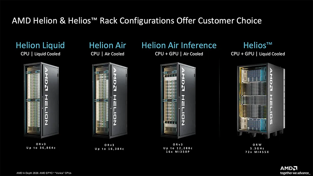
(1) Helion Liquid: Designed to operate alongside AMD Helios rack-scale systems in large agentic AI deployments. This configuration prioritizes agent density and uses liquid cooling. At a rack power level of 120kW, it supports 36,864 cores and 73,728 threads, with capacity for more than 73,000 agents per cabinet.
-
(2) Helion Air: Aimed at data centers that use air cooling. The system provides more than 16,000 cores and can host over 32,000 agents at approximately 60kW of rack power.
-
(3) Helion Air Inference: Combines CPU execution with local GPU inference in the same rack. This arrangement allows models and their associated tools to run locally and concurrently.
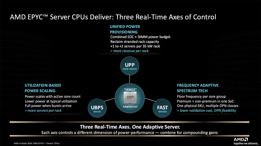
Power allocation becomes especially important when operators want to maximize the number of agents inside a rack with a fixed power limit. AMD addresses this with Unified Power Provisioning (UPP), which coordinates the power budgets of the CPU and memory.
The CPU and memory do not always reach their peak power consumption at the same time. UPP uses that difference to redistribute available power. For example, when memory needs more power, the system can apply a power cap to the CPU. AMD says enabling UPP can improve performance by 20% within the same overall power budget.
The Helion rack blueprint is designed as an open infrastructure approach rather than a fixed configuration. Customers can select CPU and GPU capacity, cooling systems, and interconnect technologies according to their deployment requirements.
AMD also provides the ROCm Agentic Toolkit for server CPUs used in agent sandboxes. The toolkit handles session management and task scheduling, while isolating tools through process-level or virtual-machine-level sandboxes on Helion systems. The goal is to simplify the deployment and scaling of agentic AI services.
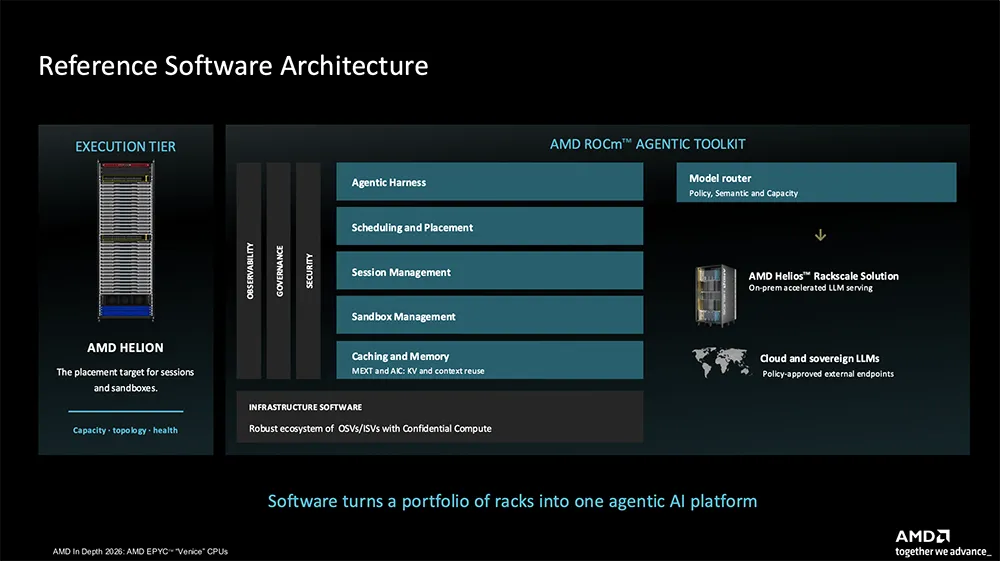
AMD says it currently has more than 10 Helion-certified rack designs. The first systems are scheduled to begin shipping in November.
For more background on the rack architecture, see AMD Helion: Open Rack Infrastructure for Agentic AI.
04. Venice SoC: Zen 6 and Zen 6c Cores, I/O Dies, and Internal Data Paths #
AMD’s design targets for Venice include high throughput, lower total cost of ownership, energy efficiency, and the enterprise features expected from a modern server platform.
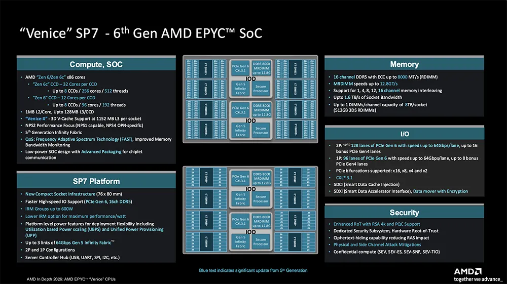
Zen 6 cores form the foundation of the Venice SP7 system-on-chip. The processor uses Core Compute Dies (CCDs), with as many as eight CCDs connected to the rest of the system through two I/O dies.
The design includes two types of CPU core:
- Zen 6: Optimized for high single-core performance and operating frequency.
- Zen 6c: Designed for higher core density and overall throughput.
Both share the same core logic and x86 instruction set, but their physical configurations differ. A high-frequency Zen 6 CCD contains 12 cores, while a high-density Zen 6c CCD contains 32.
With up to eight CCDs, the SoC can scale to 96 Zen 6 cores or 256 Zen 6c cores. Both configurations support Simultaneous Multi-Threading (SMT), providing up to 192 or 512 threads, respectively.
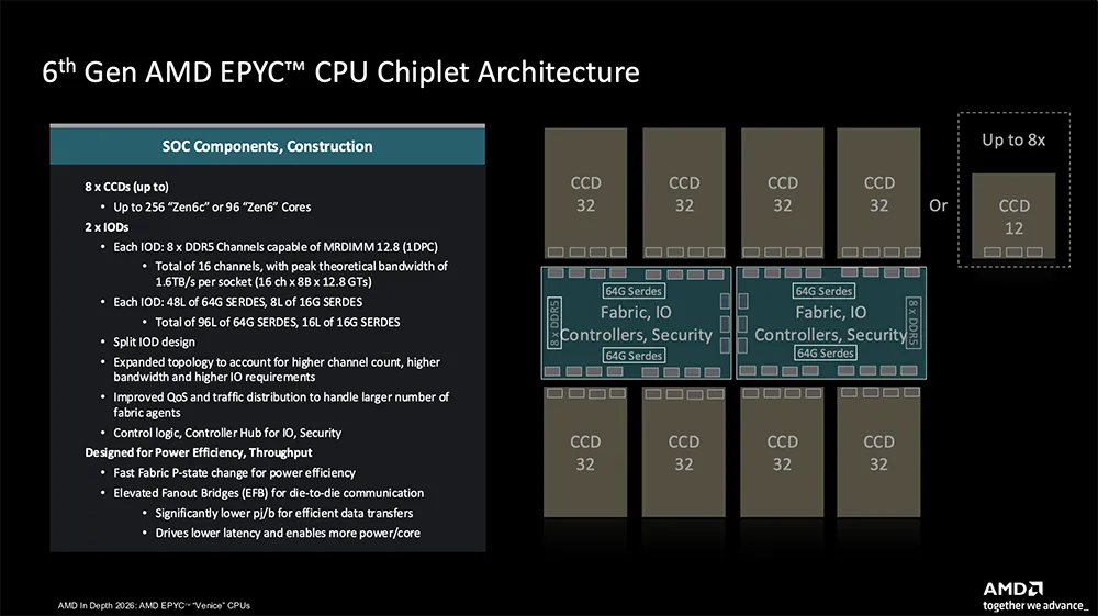
The I/O dies handle much of the functionality outside the CPU cores. The two dies share the same physical design and are rotated 180 degrees relative to each other inside the package.
Each I/O die contains eight DDR5 memory channels and 48 PCIe 6.0 channels, along with control logic, power-management modules, I/O hubs, and secure microcontrollers.
The 5th Gen Infinity Fabric connects the different parts of the SoC. It routes requests to the appropriate CCD, memory controller, or I/O port while managing traffic and Quality of Service (QoS). These routing and control mechanisms help ensure that CPU cores receive data while maintaining the requirements of different traffic types.
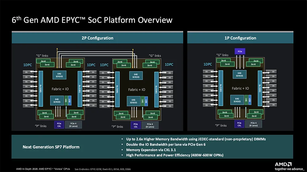
To keep the larger core configurations supplied with data, AMD has increased the number of Scalable Data Ports (SDP).
A 32-core CCD includes four SDP ports, while a 12-core CCD includes three. Each port provides 32 bytes of read bandwidth and 16 bytes of write bandwidth per cycle.
AMD has also redesigned the package-level connections between the CCDs and I/O dies. The new Advanced Fan-Out Bridge (EFB) technology brings the dies to within a few hundred micrometers of one another, reducing connection distance, power consumption, and latency.
The packaging process begins by forming copper pillars on a glass carrier and positioning the bridge chips. The structure is then molded, followed by the creation of redistribution layers (RDL) that route signals to micro-bumps. Active dies are attached before the reconstructed module is separated into individual packages.
The use of two I/O dies also makes system topology more important. The physical placement of threads and data can affect memory access paths, so AMD uses NPS (Nodes Per Socket) to organize compute, memory, and I/O resources into proximity domains.
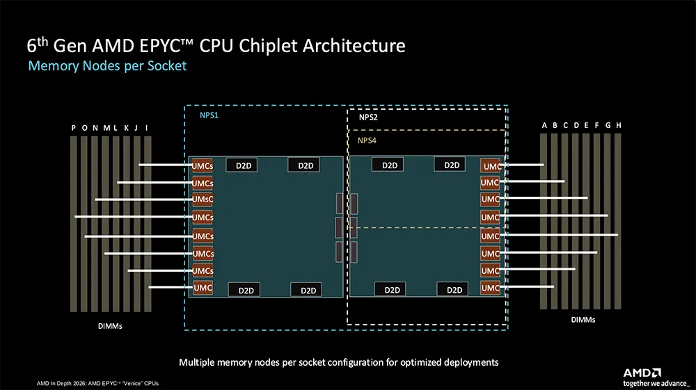
NPS1 interleaves memory access across all 16 channels. This is useful when software cannot precisely control where threads and data are placed.
NPS2 divides the socket into two NUMA domains aligned with the I/O dies. Each domain can contain up to 128 cores and eight memory channels. With full-speed MRDIMMs, a single domain provides approximately 819 GB/s of theoretical memory bandwidth. AMD notes that this exceeds the total memory bandwidth of an entire previous-generation Turin SoC.
NPS4 divides the resources into four domains. This arrangement can be useful when a server needs to run several independent parallel workloads within one socket.
As the SoC grows, NPS2 offers a practical balance between the available compute resources and the memory bandwidth accessible within each domain.
05. Zen 6c: Major Microarchitecture Changes Over Zen 5c #
CPU microarchitecture design involves balancing four major factors: operating frequency, instructions per cycle (IPC), power consumption, and die area. Improving one area can affect the others, so AMD has progressively developed different core configurations to address different server workloads.
For Zen 6, AMD identifies five main design goals:
- Improve single-core performance.
- Deliver higher overall throughput efficiently.
- Expand AI-related capabilities for agentic workloads.
- Improve performance at low-latency operating points.
- Strengthen trusted computing features.
AMD continues to optimize the relationship between frequency and IPC. Zen 6c targets a lower operating frequency than the high-frequency Zen 6 design, allowing AMD to allocate more internal resources to each core and improve IPC.
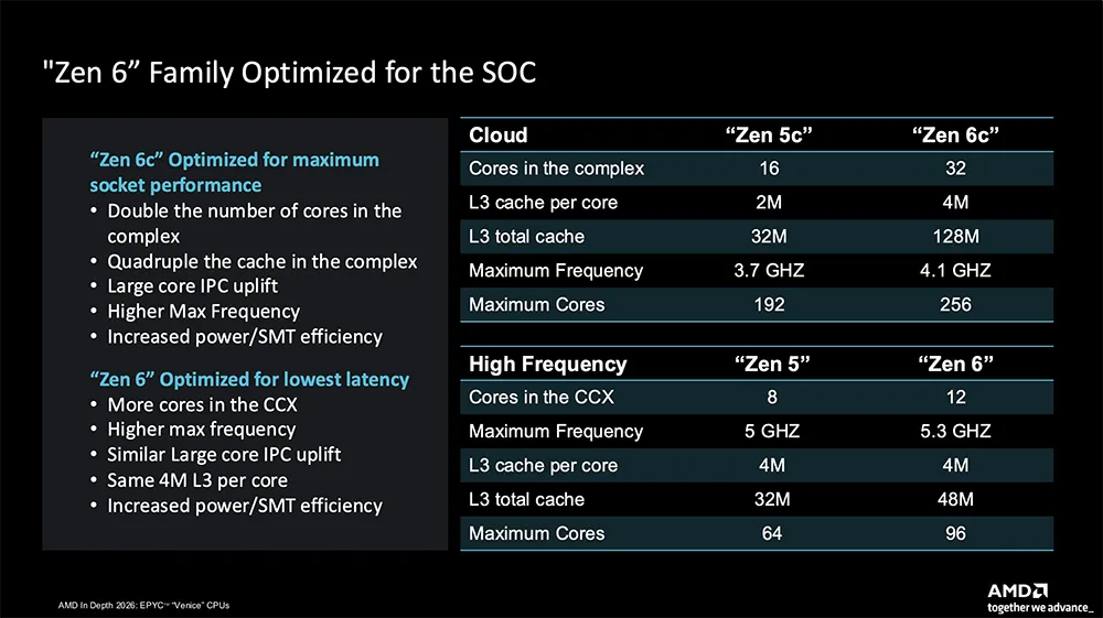
Compared with Zen 5, the Zen 6 CCD increases its core count to 12, raises maximum frequency to 5.3 GHz, and expands L3 cache to 48 MB. The complete processor can scale to 96 cores.
Zen 6c makes a different set of changes compared with Zen 5c. Its CCD doubles the core count to 32, while per-core L3 cache increases from 2 MB to 4 MB. That gives each 32-core CCD a total of 128 MB of L3 cache. Maximum frequency rises to 4.1 GHz, and the full processor can scale to 256 cores.
The larger core complex can keep more workloads within a single cache-coherent domain. This can benefit large virtual machines and multithreaded applications whose threads frequently share data.
Under fixed-frequency, light-load testing conditions, AMD reports the following average IPC improvements for Zen 6c over Zen 5c:
- Approximately 20% for enterprise and cloud server workloads.
- Approximately 31% for AI workloads.
- Approximately 27% across the combined workload set.
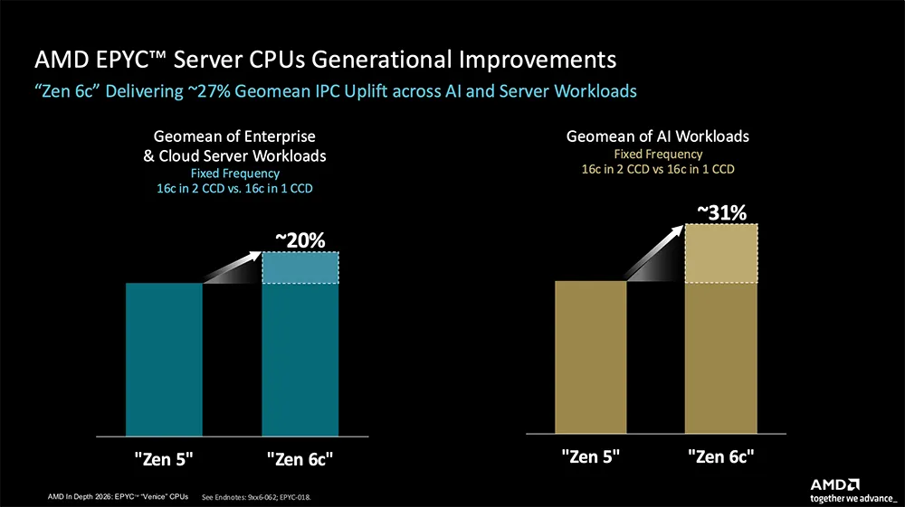
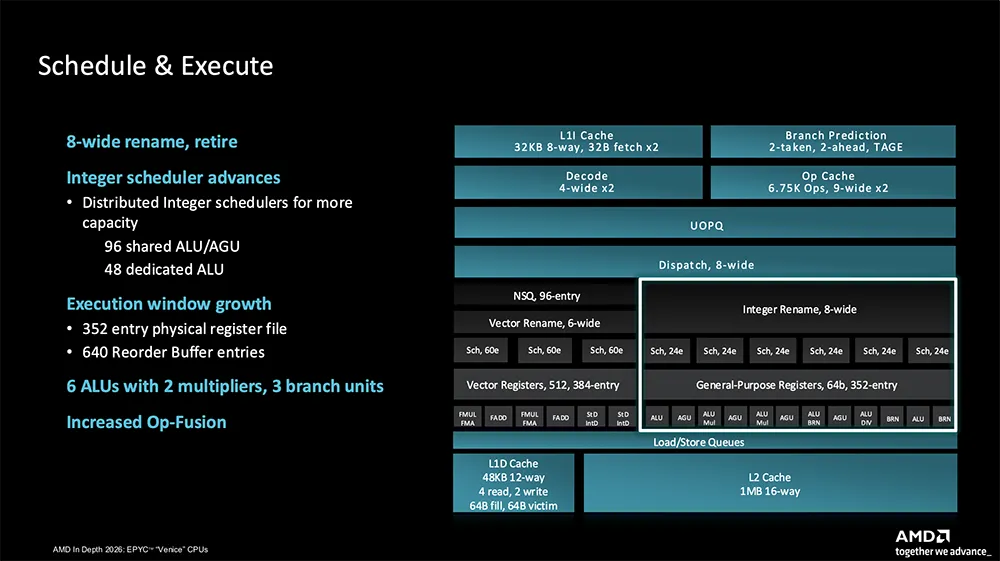
AMD attributes these gains to a series of changes throughout the core.
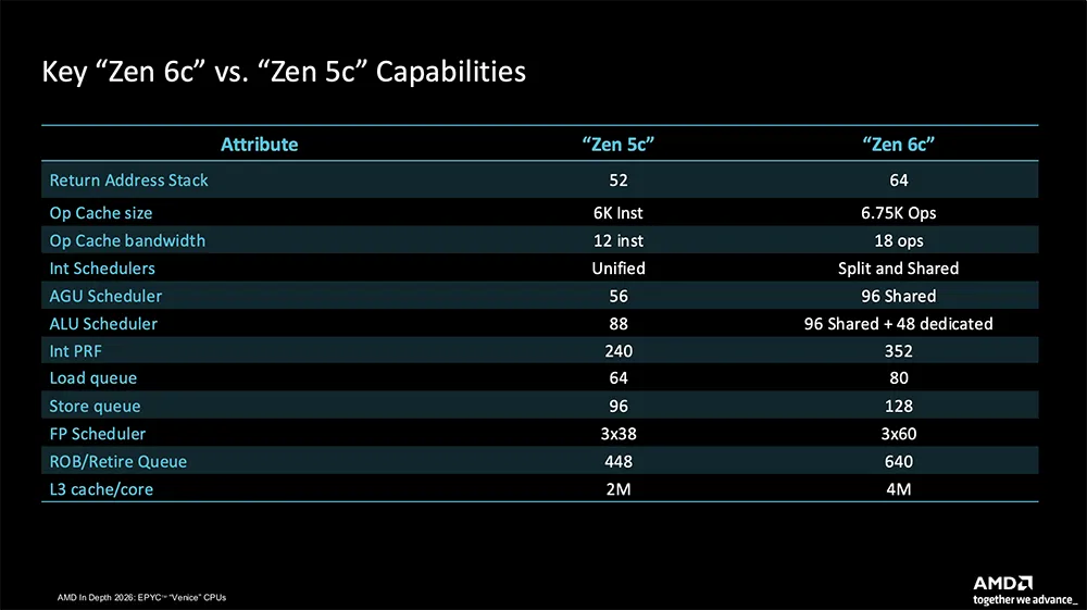
The major Zen 6c improvements over Zen 5c include:
- Branch Target Buffer (BTB): The return address stack grows from 52 to 64 entries.
- Op Cache: Capacity increases from 6K to 6.75K operations.
- Op Cache bandwidth: Throughput increases from 12 to 18 instructions per cycle.
- Integer scheduler: The unified design is replaced by a distributed and shared arrangement. Address Generation Units (AGUs) and Arithmetic Logic Units (ALUs) share a 96-entry scheduler pool, with another dedicated 48-entry pool for ALUs handling heavier integer workloads.
- Integer physical register file: Capacity increases from 240 to 352 entries.
- Load queue: Capacity increases from 64 to 80 entries.
- Store queue: Capacity increases from 96 to 128 entries.
- Floating-point scheduler: Capacity expands from 3 × 38 to 3 × 60 entries.
- Reorder Buffer (ROB): Capacity grows from 448 to 640 entries.
- L3 cache: Average L3 capacity per core doubles from 2 MB to 4 MB.
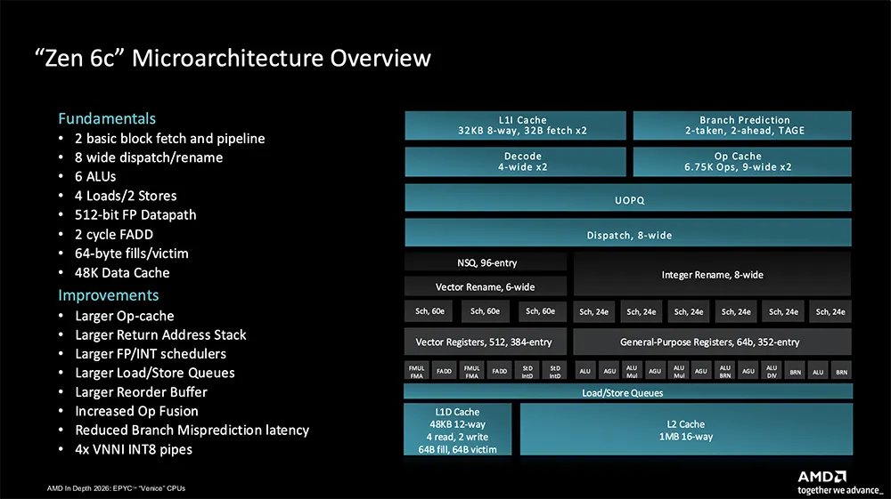
Zen 6 also improves branch prediction accuracy and reduces prediction latency. Micro-op fusion has been expanded as well. This technique combines two instructions into a single micro-op, allowing certain instruction pairs to use one scheduling and result-forwarding slot rather than two.
Reducing the number of micro-ops needed for some operations can improve both execution efficiency and power consumption. It also allows more instructions to remain in flight without requiring a corresponding increase in the physical ROB.
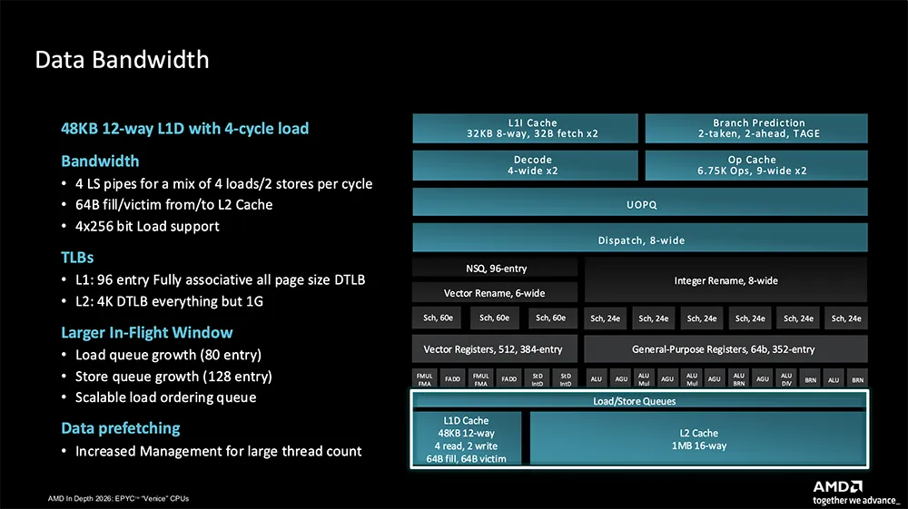
The cache and memory subsystem receives several changes involving bandwidth, Translation Lookaside Buffers (TLBs), instruction windows, and data prefetching.
The bandwidth between L3 and L2 remains 32 bytes per cycle, while the L2-to-L1 path provides 64 bytes per cycle.
The L1 TLB uses a fully associative design across page sizes. The L2 TLB provides a large-capacity structure for 4KB pages and supports all page sizes except 1GB pages, which use a separate dedicated TLB.
Prefetching behavior also needs to adapt to different workloads. A lightly loaded CPU and a system with many active threads do not necessarily benefit from the same prefetch strategy. AMD has therefore tuned the algorithms to adjust their behavior according to active workloads and changes in system activity.
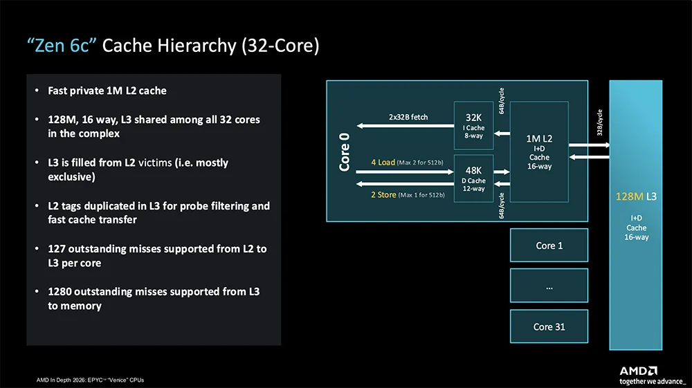
Zen 6 and Zen 6c share the same general cache hierarchy, with some differences in queue capacity. Zen 6c provides 4 MB of L3 cache per core and maintains full cache coherence across its 32-core complex.
The L3 cache uses a victim-cache design, receiving data evicted from L2. Shadow tags help determine whether requested data is already present in another core’s cache. As a result, an L3 miss does not always require a trip to external memory; the data may still be available elsewhere within the core complex.
The 32-core configuration can support up to 1,280 concurrent uncompleted hit requests from L3 toward memory, compared with 480 in the 12-core version with 48 MB of L3 cache.
Under heavy system-wide load, the prefetcher also adjusts its behavior to avoid redundant requests consuming bandwidth that could be used by demand traffic.
06. Zen 6 Instructions: Native FP16 and More VNNI INT8 Capacity #
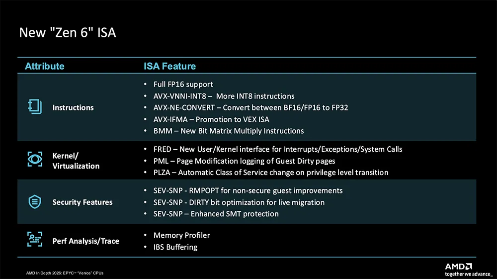
AMD continues to extend the x86 instruction set with each new processor generation. Zen 6 adds full FP16 support, incorporates newer AVX instruction additions also introduced by Intel, and expands support for selected data conversion and VEX-encoded IFMA operations.
Zen 6 maintains two 512-bit load operations per cycle while supporting four 256-bit load operations per cycle. This is useful for software that already uses 256-bit AVX instructions but is difficult to vectorize further. Such code can make better use of the available load bandwidth without requiring a complete rewrite around wider vectors.
FP16 execution is another important change.
Zen 5 supports FP16 format conversion, but applications may need to convert data to FP32, perform calculations, and then convert the results back to FP16. Those conversion steps introduce additional work.
Zen 6 and Zen 6c add native AVX-512 FP16 compute support, allowing compatible workloads to perform FP16 operations directly.
AMD has also expanded the VNNI INT8 execution pipelines used by AI workloads. Zen 5 has two lanes, while Zen 6 increases that number to four.
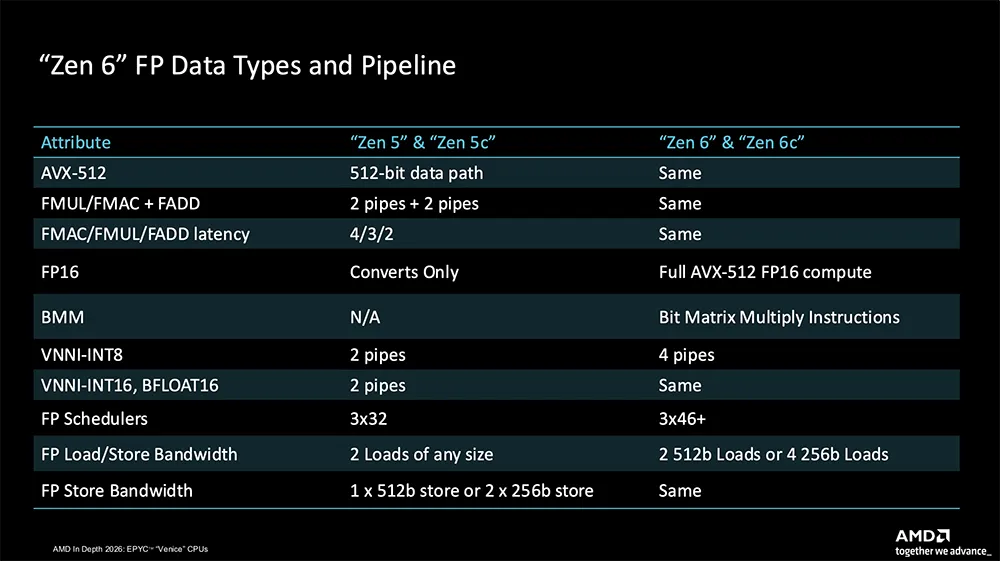
Zen 6 also introduces BMM (Bit Matrix Multiply), a new instruction capability for bit-level operations. Its intended uses include cryptographic algorithms, AI workloads, and other applications that rely heavily on bit manipulation.
There are also differences between the two core designs. The high-frequency Zen 6 core has a 46-entry floating-point scheduler, while Zen 6c uses a 60-entry scheduler. This reflects their different priorities: Zen 6 emphasizes frequency headroom, while Zen 6c uses a wider execution window to find more instruction-level parallelism.
For operating systems and virtualization, Zen 6 adds FRED (Flexible Return and Event Delivery). FRED provides a new interface for handling interrupts, exceptions, and system calls across user and kernel space. AMD says the feature can improve performance and security while simplifying implementation for operating-system and hypervisor developers.
Performance profiling also receives new capabilities. Zen 6 adds a standalone memory profiler and hardware buffering for Instruction-Based Sampling (IBS).
The memory profiler uses dedicated registers and tracking mechanisms to monitor memory-subsystem activity. With IBS buffering, sample data can be written automatically into memory buffers, reducing the interrupt overhead associated with collecting performance samples.
07. Memory Architecture: DDR5, LPDDR5X, and CXL 3.1 #
Venice supports several memory technologies to address different requirements for bandwidth, capacity, and power consumption.
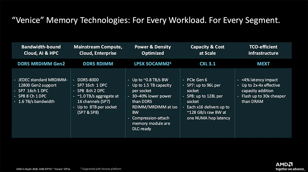
The first option is DDR5. The SP7 platform provides 16 DDR5 memory channels using a one-DIMM-per-channel configuration.
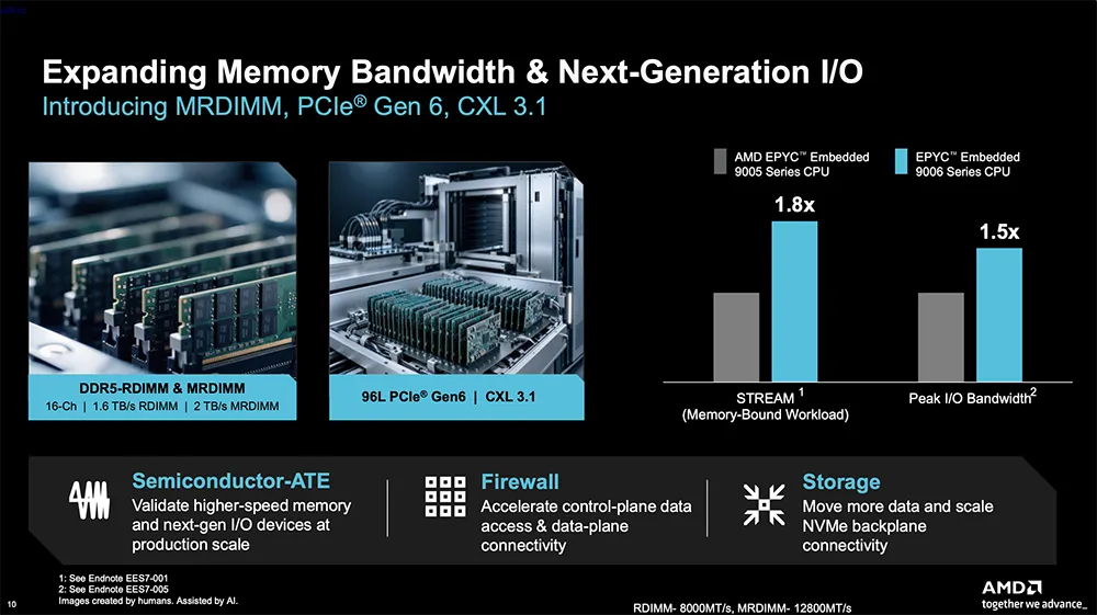
With DDR5-8000 RDIMMs, the theoretical bandwidth across all channels reaches approximately 1.02 TB/s. Using 12.8 GT/s MRDIMMs raises the theoretical figure to approximately 1.64 TB/s. Capacity can reach 8 TB with sixteen 512 GB DIMMs.
Verano uses a more power-conscious LPDDR5X design. Its memory interface is divided across four independent memory dies, each with six channels. Together, they provide 24 channels and a 768-bit interface through interchangeable SOCAMM modules.
The design uses N2 for the compute dies, N3 for the memory dies, and N6 for the I/O dies. For AI host nodes that need to keep SoC power below 400W, reducing memory-side power consumption can leave more of the available budget for CPU cores.
CXL 3.1 and MEXT provide two additional ways to expand the memory hierarchy.
CXL allows memory attached to external devices to be mapped into the system address space. This can be used for capacity expansion, software-defined memory tiering, or interleaving. With DRAM prices putting pressure on server budgets, CXL can also help customers reuse investments in older memory technologies and build terabyte-scale memory configurations at a lower cost.
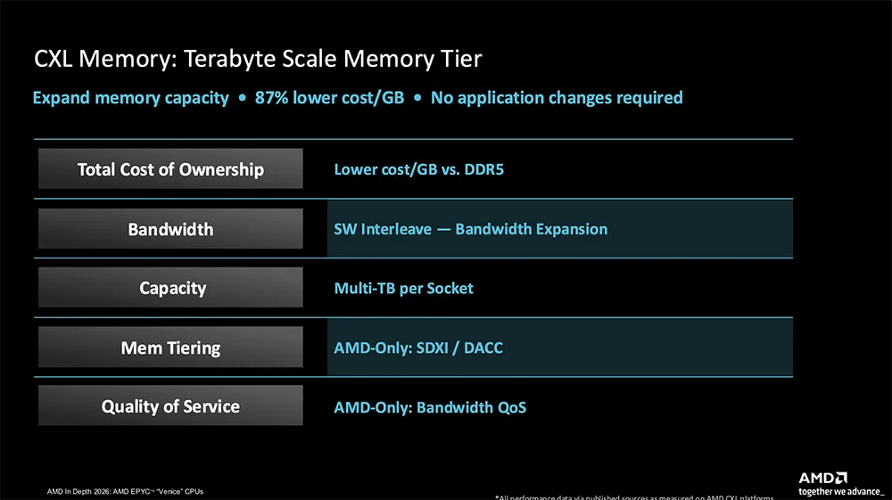
All 96 PCIe channels on Venice natively support CXL. AMD says users do not need to preconfigure the platform: when a compatible device is connected, the system identifies it as either a PCIe or CXL device.
Platform QoS mechanisms distinguish local DDR traffic from CXL traffic to help reduce bandwidth contention between the two.
MEXT is a separate memory optimization technology that AMD acquired in June. It aims to reduce DRAM waste by using flash storage as an additional tier in the memory hierarchy. Given the cost of high-capacity server memory, this is one of the more significant technologies AMD discussed during the briefing.
08. MEXT: Using Flash to Reduce DRAM Requirements #
MEXT began working with AMD as early as 2024. AMD described an internal deployment involving 145 systems that used MEXT memory tiering to increase available memory capacity. The resulting DRAM procurement savings reached $4.9 million, which AMD said represented 83% of the cost of a single system.
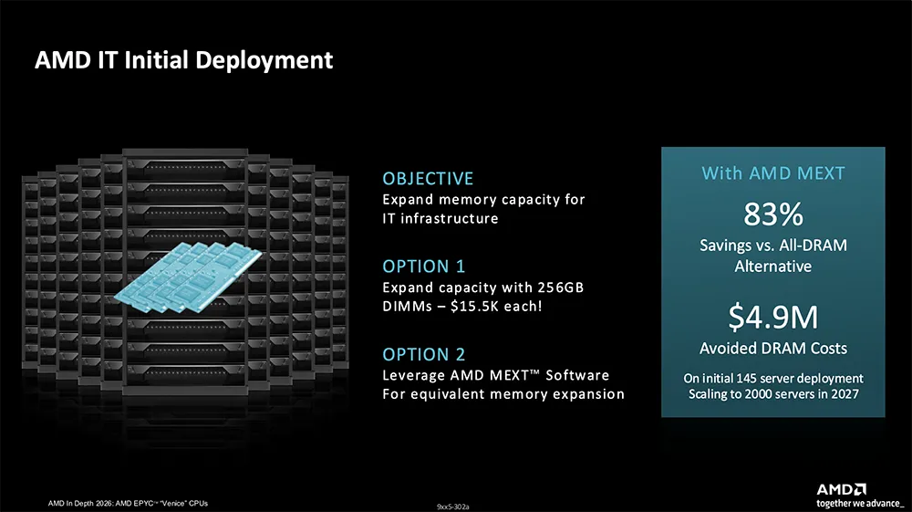
The central idea behind MEXT is to use software and predictive algorithms to make better use of the memory already installed in a server.
The software monitors system activity and uses AI to predict which memory pages are likely to be accessed soon. It can then move those pages from flash storage into DRAM before an application requests them.
In practical terms, frequently accessed data stays in DRAM, while less active data can reside on NVMe flash. The application continues to use the system’s memory interface without needing to manage the movement of individual pages itself.
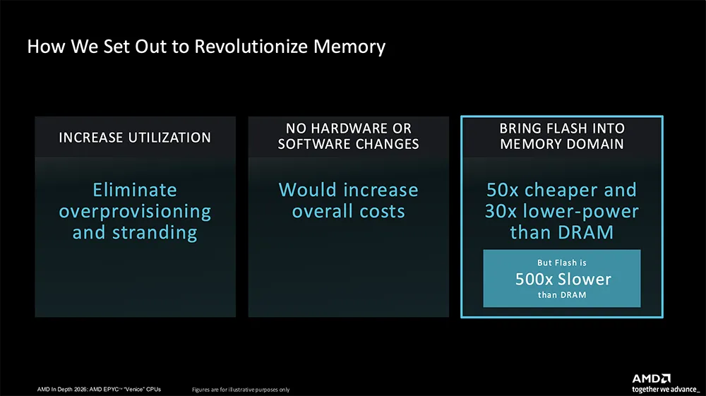
Flash is attractive because its cost and power consumption per bit are much lower than DRAM. AMD’s presentation compares the technologies as follows:
- Flash costs approximately 1/50 as much per bit as DRAM.
- Flash consumes approximately 1/30 as much power per bit.
- Flash access speed is approximately 1/500 of DRAM.
The trade-off is clear: flash offers much cheaper capacity, but it cannot replace DRAM for every memory access. The effectiveness of tiering depends on how accurately the software identifies the pages that applications will need.
MEXT is implemented in software. Its components include Linux drivers, AI inference engines, and the RAMView tool, which provides visibility into real-time memory usage.
According to AMD’s presentation, MEXT can train in approximately one second using a single EPYC CPU core. Its predictions are expected to improve as the system continues running and gathers more workload information.
The financial benefit comes from reducing the amount of expensive DRAM required in each server.
For example, a customer planning to purchase a server with 2 TB of DRAM could instead install 1 TB of DRAM and use MEXT with NVMe flash to provide additional memory capacity.
DIMM pricing creates another potential saving. Reaching 2 TB of DRAM may require expensive 256 GB modules. A configuration using 128 GB DIMMs can cost considerably less than half the price of an equivalent capacity built from 256 GB modules. Combining smaller DIMMs with flash-backed tiering can therefore reduce the memory budget further.
MEXT can also extend the usable memory capacity of existing servers. A system with 1 TB of physical DRAM could use software and NVMe flash to present 1.2 TB, 1.5 TB, 2 TB, 3 TB, or even 4 TB of system memory.
The technology is intended for several deployment environments, including on-premises enterprise data centers, cloud systems, virtual machines, bare-metal servers, and containers. AMD says both new and previously deployed EPYC servers can use it, provided they have suitable NVMe drives or available drive bays.
AMD’s MEXT software is designed to reduce DRAM requirements progressively, starting with a full-DRAM configuration and moving through reductions of 25%, 50%, and beyond.
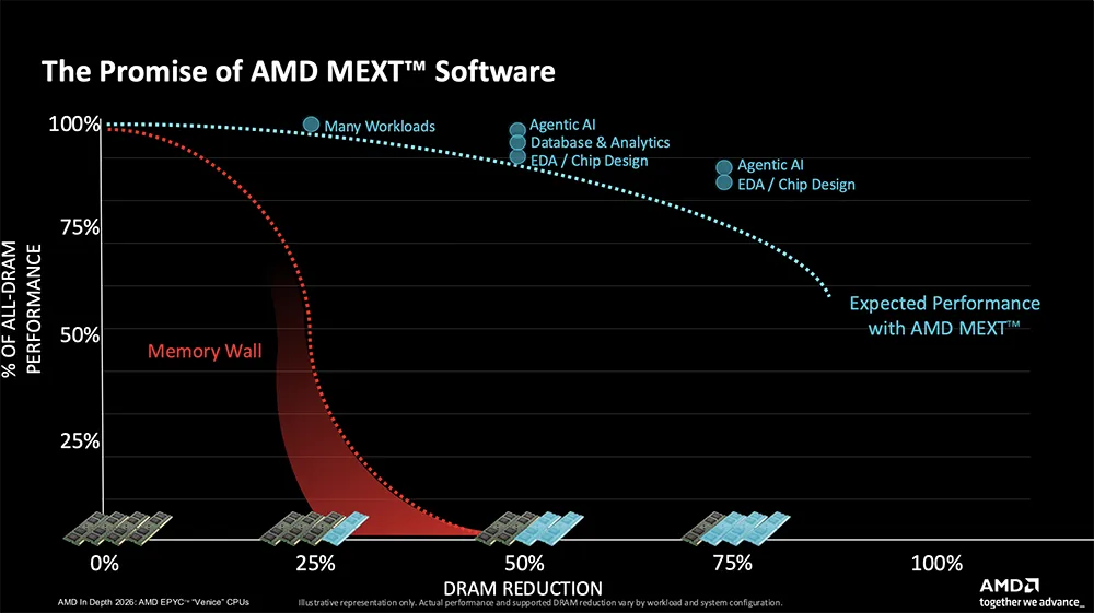
AMD presented results from agentic AI, database analytics, and electronic design automation (EDA) workloads. In five agent workloads, cutting DRAM capacity in half while using MEXT retained 99% of the performance of the full-DRAM baseline.
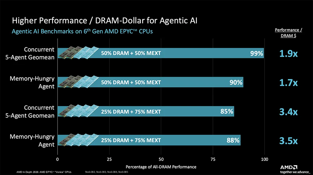
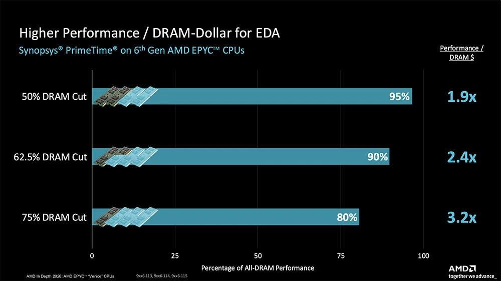
The presentation also showed results with DRAM capacity reduced to one-quarter of the original configuration. For Synopsys PrimeTime EDA workloads running on Venice, a configuration with half the original DRAM retained 95% of full-DRAM performance.
In an Apache Spark test running on Microsoft Azure infrastructure, halving DRAM capacity while using MEXT retained 99% of the performance of the original configuration.
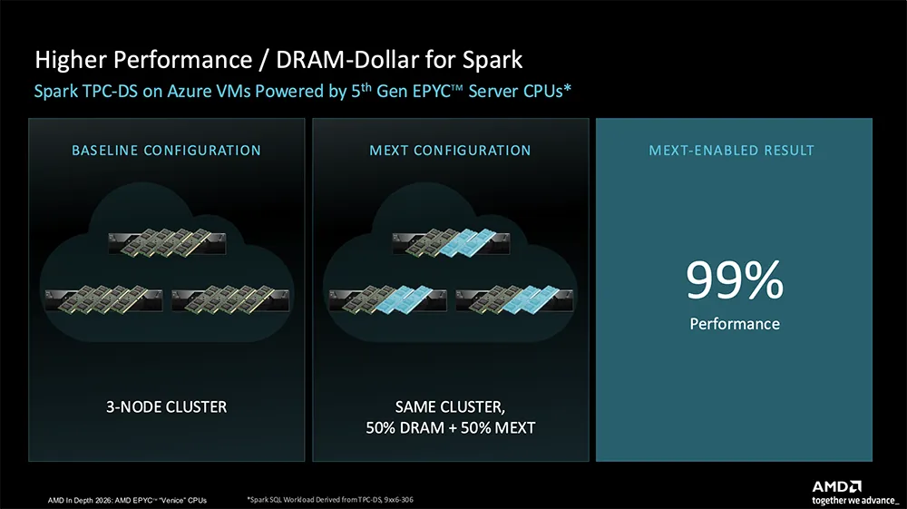
These results suggest that memory tiering could help reduce server acquisition costs for workloads that do not need every active memory page to reside in DRAM. Actual results will depend on access patterns, prediction accuracy, flash performance, and the amount of memory pressure in each application.
09. PCIe 6.0 and SDXI: Improving Data Movement #
Venice upgrades the platform to PCIe Gen 6, increasing the per-lane signaling rate to 64 GT/s. The standard also introduces Forward Error Correction (FEC), updated signaling methods, and FLIT modes to improve transmission efficiency.
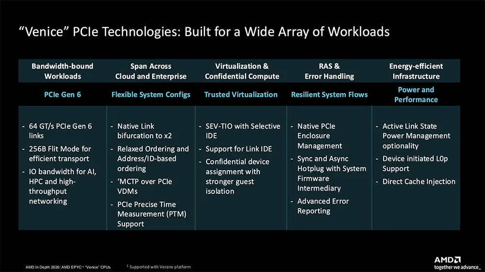
A single-socket SP7 system supports up to 96 PCIe Gen 6 lanes, along with an additional eight PCIe Gen 4 lanes. Dual-socket configurations support up to 128 PCIe Gen 6 lanes and 16 PCIe Gen 4 lanes.
AMD has also made changes to the data paths connecting PCIe devices to the CPU. Precision Time Measurement (PTM) helps synchronize time bases between processor ports and PCIe devices.
For virtualization and confidential computing, Venice supports PCIe Link IDE (Integrity and Data Encryption). The platform also retains hot-plug support and Advanced Error Reporting (AER).
PCIe Gen 6 includes more flexible link power management. Its L0p low-power state allows a link to remain active while reducing its operating power. Transmission capacity can then increase again when demand rises.
Direct cache injection is another way to shorten the path between devices and CPU execution. Instead of requiring the processor to retrieve data through a conventional memory path, compatible devices can inject data directly into cache.
Venice supports this mechanism for devices that provide TLP Processing Hints (TPH). The platform can also provide cache injection for selected devices that do not support TPH.
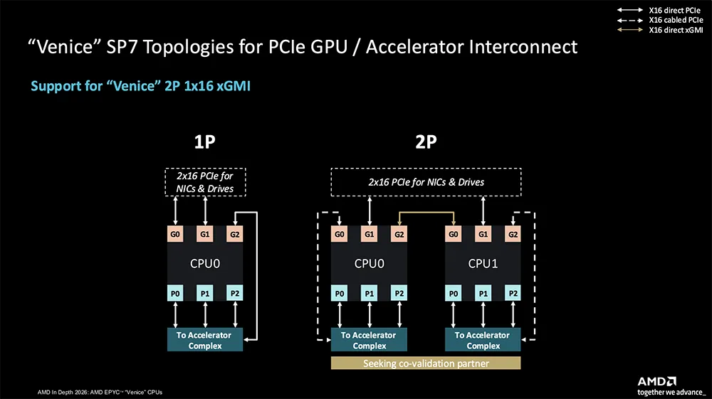
For dual-socket systems, customers can choose between two or three xGMI links according to their NUMA and I/O requirements. More links dedicated to socket-to-socket communication provide greater inter-socket bandwidth. Using fewer links for that purpose leaves more resources available for peripherals.
Venice also includes the SDXI Data Movement Engine, which can offload memory-copy, memory-zeroing, and encryption operations from the CPU.
AMD estimates that SDXI can deliver approximately 100 GB/s of data movement throughput and around 50 GB/s of cryptographic acceleration throughput.
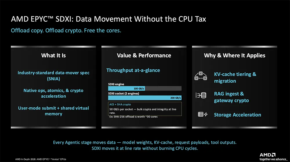
The engine supports virtualization as well. Administrators can configure it as an SR-IOV-enabled device and assign its functions to specific guest virtual machines. This allows virtualized workloads to access data movement and cryptographic acceleration without relying entirely on the host CPU.
10. Power Management: DFP, UPP, UBPS, and FAST #
As server processors add more cores, power consumption outside the CPU cores becomes increasingly important. Fabric interconnects, memory controllers, and other SoC components all contribute to the platform’s overall power budget.
AMD addresses this with Dynamic Fabric Power (DFP), a mechanism that changes fabric operating frequency according to workload requirements. Latency-sensitive tasks can trigger higher fabric frequencies, while less demanding conditions allow the system to reduce frequency and power consumption.
AMD says the new design also shortens power-state transition latency, reducing the periods in which data movement could otherwise stall.
Data center operators face three related power-management challenges:
- Recovering power capacity that would otherwise remain unused.
- Adjusting power allocation as workloads change.
- Maintaining performance when the system reaches power or thermal limits.
AMD’s Venice platform uses three technologies to address these requirements.
-
(1) UPP (Unified Power Provisioning): Treats the CPU SoC and DIMMs as a combined power-budgeting unit. Their peak power demands do not always occur at the same time, so UPP can reduce excess power headroom reserved for each component. AMD says this can lower platform power-capacity planning requirements by approximately 10% to 15%.
-
(2) UBPS (Utilization-Based Power Scaling): Adjusts power allocation according to system utilization. When workloads become more active, the system can use available headroom to support higher voltage and frequency levels, balancing performance against power consumption.
-
(3) FAST (Frequency-Adaptive Spectrum Technology): Assigns performance priority classes to CPU cores. When the system reaches a power or thermal limit, lower-priority cores are reduced in frequency first, helping protect the response time of more critical threads.
These technologies can be used together. Customers can profile the power and performance characteristics of their systems and choose settings that match their workloads and operating constraints.
11. RAS and Security: Fault Isolation and Confidential Computing #
Reliability, Availability, and Serviceability (RAS) are fundamental requirements for data center processors. A server platform must be able to detect faults, isolate affected components, and recover without unnecessarily disrupting the rest of the system.
Venice supports PCIe Advanced Error Reporting and CXL 3.1 device fault recovery. Its memory RAS features retain Chipkill-grade reliability protection and add improvements to Machine Check Architecture error logging.
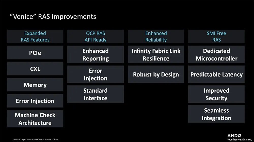
AMD is also working with the Open Compute Project (OCP) to improve the APIs used by its RAS ecosystem while reducing reliance on SMI and SMM mechanisms.
Venice introduces MPRAS, which uses dedicated on-chip microcontrollers to handle tasks that previously required System Management Interrupts. Moving this work away from SMI can reduce interruptions to business workloads.
Interconnect reliability receives additional protection through link encryption, forward error correction, and CRC checks.
Security is another major part of the Venice platform. AMD combines a dedicated security subsystem with flexible confidentiality controls and hardware features intended to support future cryptographic requirements.
The processor includes RSA-4096 integration as part of its preparation for Post-Quantum Cryptography (PQC). It also supports Calyptra 1.2 Root of Trust, which helps establish a hardware trust foundation for AI workloads and gives customers more control over platform security.
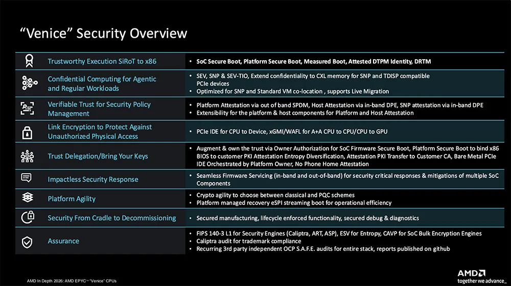
For confidential computing, Zen 6 extends SEV-SNP (Secure Encrypted Virtualization-Secure Nested Paging) with RMPOPT, DIRTY bit optimizations, and improved SMT protection.
These changes are intended to reduce inspection overhead when secure and non-secure virtual machines share a system, simplify live VM migration, and preserve isolation while making use of SMT performance.
Venice also supports SEV-TIO. This combines PCIe link encryption with TDISP to allow qualified devices to participate in Trusted Execution Environments. For deployments that need link-level protection without the broader confidential-computing setup, PCIe IDE can operate independently to provide encryption and integrity protection.
AMD has also introduced device provenance verification. This approach cryptographically connects hardware bill-of-materials information from manufacturing to the identity of the processor. Customers can use that relationship to trace device lineage, verify authenticity and integrity, and improve security audit transparency through OCP S.A.F.E.
The 6th Gen EPYC family reflects AMD’s view that server CPU requirements are becoming increasingly diverse. Rather than relying on one configuration for every workload, the company is building around a shared microarchitecture and a set of core and platform designs optimized for different operating points.
Zen 6 targets high-frequency applications, while Zen 6c emphasizes core density. Different socket and memory configurations extend the family into enterprise systems, HPC, GPU host nodes, and AI infrastructure.
AMD is also expanding its optimization efforts beyond the processor itself. Helion addresses rack-level deployment, UPP coordinates power across CPUs and memory, and MEXT aims to reduce the amount of expensive DRAM required by using flash as another tier in the memory hierarchy.
That broader approach is particularly relevant as data center operators face rising memory costs and growing demand for CPU resources in agentic AI systems. Venice is designed to function as a general-purpose server processor while also serving as a foundation for larger AI deployments.