Huawei Tau Scaling: How LogicFolding Targets Chip Power and Heat
Huawei semiconductor executive He Tingbo has published a new paper addressing one of the most obvious challenges surrounding the company’s proposed Tau (τ) scaling law: thermal management.
Titled Huawei’s τ Chip Was Supposed to Melt?, the paper argues that increasing transistor density through vertical integration does not necessarily translate into higher operating temperatures.
The central argument is that modern SoCs increasingly spend a substantial portion of their dynamic power moving data through interconnects rather than performing computation in transistor logic itself.
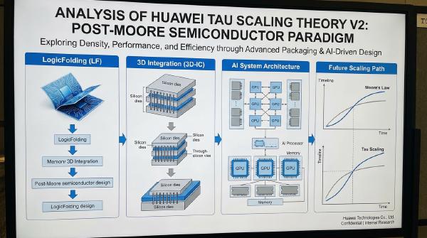
Huawei’s proposed solution is LogicFolding: vertically reorganizing portions of a chip so that signals travel shorter distances through dense hybrid-bonded connections instead of crossing long horizontal interconnects.
According to the paper, the approach has already been applied to the company’s claimed Kirin 2026 design.
Huawei says the chip increases transistor density by approximately 55% compared with its predecessor while reducing power consumption under selected iso-performance workloads by up to 66%.
The broader objective is not simply to stack more silicon.
It is to use the additional physical dimension to shorten signal paths, reduce interconnect capacitance, create additional parallelism, and ultimately operate workloads at lower voltage and power.
That makes the thermal argument surrounding Tau scaling considerably more nuanced than the simple assumption that:
More transistors per square millimeter = more heat per square millimeter.
🔥 The Thermal Objection to 3D Integration #
Three-dimensional integration has long promised a way to increase system density without relying entirely on conventional planar scaling.
But stacking active silicon introduces an obvious problem.
If two layers of active circuitry occupy approximately the same footprint, the amount of heat generated inside that footprint can increase substantially.
Heat generated inside a lower layer must also travel through additional material before reaching a cooling interface.
The conventional argument is therefore straightforward:
More Active Layers
       │
       ▼
More Transistors / Area
       │
       ▼
Higher Power Density
       │
       ▼
More Heat
       │
       ▼
Higher Junction Temperature
       │
       ▼
Throttling / Reliability Limits
This is the concern He Tingbo’s latest paper attempts to address.
Huawei’s argument is that this model focuses too heavily on transistor density while underestimating the amount of power consumed by data movement.
If vertical integration significantly reduces the distance that signals travel, the additional transistor density can potentially be accompanied by lower dynamic power.
That is the central thesis behind LogicFolding.
⏱️ What Is the Tau Scaling Law? #
Huawei introduced the concept of Tau (τ) scaling as a different way of thinking about semiconductor scaling.
Traditional semiconductor scaling primarily focuses on reducing physical dimensions.
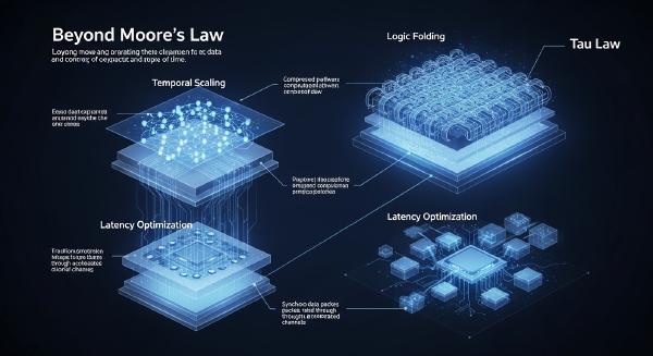
The Tau approach instead emphasizes reducing the characteristic latency associated with signal propagation through a system.
In simplified form:
Traditional Scaling
      │
      ▼
Smaller Transistors
      │
      ▼
Shorter Physical Dimensions
      │
      ▼
Higher Speed / Lower Power


Tau Scaling
      │
      ▼
Shorter Critical-Path Latency
      │
      ▼
Reduced Signal Travel Distance
      │
      ▼
Higher System Efficiency
Huawei positions τ as a system-level engineering principle, rather than simply another transistor architecture.
LogicFolding is one implementation of that broader concept.
The basic idea is to reorganize circuits that would traditionally occupy a single planar layer across multiple vertically stacked silicon layers.
Instead of making every transistor physically smaller, the architecture attempts to make the communication paths between those transistors shorter.
🧩 LogicFolding: Trading Space for Time #
LogicFolding can be understood as a form of three-dimensional circuit reorganization.
Consider a conventional planar circuit:
A ───────────────────────────────► B
       Long horizontal path
The same logic can potentially be reorganized vertically:
Layer 1
A
│
│
▼
Vertical Interconnect
│
▼
Layer 2
B
The signal now travels through a short vertical connection instead of crossing a long horizontal route.
The objective is not simply to stack arbitrary circuits.
Huawei says its engineers identify particularly long and power-hungry signal paths within blocks such as:
- NPU
- GPU
- CPU
- DSP
Those paths are then candidates for vertical reorganization.
The expected benefits include:
- Shorter interconnects
- Lower capacitance
- Reduced signal-transition energy
- Lower clock-routing overhead
- Greater transistor density
- Additional space for parallel execution units
- Potentially lower operating voltage
The key is that LogicFolding attempts to improve both physical layout and system architecture simultaneously.
🔗 Hybrid Bonding Is the Enabling Technology #
The physical foundation of the approach is 3D hybrid bonding.
Rather than connecting stacked dies through relatively large conventional package-level interconnects, hybrid bonding can create extremely dense direct connections between silicon structures.
The general process involves aligning two surfaces, bringing them into contact, and applying thermal treatment so that the materials form permanent bonds.
Copper interconnect structures on the opposing surfaces provide electrical connections between the layers.
Conceptually:
Top Silicon Layer
────────────────────────
● ● ● ● ● ● ● ●
│ │ │ │ │ │ │ │
════════════════════════
Hybrid Bond Interface
════════════════════════
│ │ │ │ │ │ │ │
● ● ● ● ● ● ● ●
────────────────────────
Bottom Silicon Layer
The smaller the bonding pitch, the more vertical connections can potentially be placed within a given area.
That matters because sparse vertical connections can force signals to fan out into longer horizontal routes.
The very problem LogicFolding is intended to solve would therefore return through the interconnect architecture.
📏 Huawei’s Reported Bonding-Pitch Roadmap #
According to the paper, Huawei reports a 1.5 μm hybrid-bonding pitch for its claimed Kirin 2026 implementation.
The design reportedly contains approximately 50 million vertical interconnects, with around 10%–15% carrying active signals.
Huawei further states that silicon for Kirin 2027 has reached a 1 μm pitch with more than 100 million vertical interconnects.
The paper describes a longer-term target of approximately 720 nm, corresponding to the cited top-metal pitch, with a future objective of exceeding 200 million vertical connections.
The proposed progression is:
Kirin 2026
1.5 μm
≈ 50M vertical connections
        │
        ▼
Kirin 2027
1.0 μm
>100M connections
        │
        ▼
Future Target
720 nm
>200M connections
        │
        ▼
Longer-Term Exploration
480 nm
These figures illustrate the importance Huawei places on bonding density.
For LogicFolding, vertical interconnects are not merely package connections.
They are effectively part of the circuit’s routing fabric.
⚡ The Hidden Power Cost: Moving Data #
The paper’s most important argument concerns dynamic power.
A simplified dynamic-power relationship is:
$$ P = \alpha C V^2 f $$
where:
- \(P\) is dynamic power
- \(\alpha\) represents switching activity
- \(C\) is effective capacitance
- \(V\) is voltage
- \(f\) is frequency
Traditional chip analysis often emphasizes transistor switching.
But interconnects also contribute substantially to capacitance.
A longer wire generally presents more capacitance that must be charged and discharged as signals transition.
That means moving data can itself become a significant energy cost.
Huawei uses an everyday analogy:
Logic gates do the work; interconnects handle the commute.
The farther the commute, the more energy is required.
LogicFolding attempts to shorten that commute.
🚗 The “Commute” Model of Chip Power #
Imagine an office where employees live hundreds of kilometers away.
Even if the work itself requires relatively little energy, transporting everyone to and from the office consumes substantial resources.
Now move everyone’s homes closer to the workplace.
The work does not change.
The transportation cost does.
Huawei argues that modern SoCs exhibit a similar effect.
Traditional SoC

Logic ──────────────── Logic
        Long Wire
           │
           ▼
      High Capacitance
           │
           ▼
     Higher Transport Cost


LogicFolding

Logic
 │
 ▼
Short Vertical Connection
 │
 ▼
Logic
 │
 ▼
Lower Transport Cost
This is the conceptual foundation for Huawei’s thermal argument.
The goal is not to reduce the amount of computation.
It is to reduce the energy required to move information between computational elements.
📉 Shorter Wires Can Reduce Dynamic Power #
According to Huawei’s reported measurements, folded signal paths were reduced by approximately 20% on average, with some critical paths shortened by as much as 70%.
Clock networks are particularly important because they distribute timing signals across large portions of the chip.
The paper claims that folding reduced clock-routing length by approximately 28% in one processing module.
It also reports a reduction in clock-buffer count from approximately 43,600 to 19,000.
The intended effect is straightforward:
Shorter Routing
      │
      ▼
Lower Effective Capacitance
      │
      ▼
Lower Dynamic Energy
      │
      ▼
Lower Power
      │
      ▼
Lower Thermal Load
This is why Huawei argues that higher transistor density does not automatically imply higher thermal density.
The additional transistor density is being used alongside architectural changes intended to reduce communication overhead.
📊 Kirin 2026: Reported Module-Level Results #
Huawei’s paper compares its claimed folded design with the previous-generation Kirin 9030 Pro under iso-performance conditions.
The important phrase is iso-performance.
The comparison attempts to hold the amount of completed work constant while measuring how much power each design requires.
According to the reported results:
| Module | Reported Power Reduction | Additional Result |
|---|---|---|
| NPU | 66% | Power density reportedly down 73% |
| GPU | 58% | Target performance at lower voltage |
| DSP | 25% | Power density initially increased 24% |
| CPU Performance Core | 41% | 9% lower clock at iso-performance |
These figures are among the most important claims in the paper because they illustrate that LogicFolding does not produce identical benefits across every circuit type.
The DSP result is particularly revealing.
A design can consume less total power while simultaneously increasing power density if its physical footprint shrinks faster than its power consumption.
That is exactly what Huawei reports for its first-generation folded DSP.
🧮 Why Power Density Can Rise Even When Power Falls #
Suppose a circuit originally consumes 100W across 100 mm²:
$$ \frac{100W}{100mm^2} = 1W/mm^2 $$Now imagine a redesigned version consumes only 75W but occupies 60 mm²:
$$ \frac{75W}{60mm^2} = 1.25W/mm^2 $$Total power decreased.
But power density increased.
This distinction is essential when discussing thermal design.
Huawei acknowledges this problem in its first-generation DSP implementation.
According to the paper, the folded DSP reduced total power by 25% while its physical area contracted by approximately 40%, producing a reported 24% increase in power density.
Huawei says the second-generation design addressed the issue, with Kirin 2027 measurements reportedly showing both lower total power and lower power density than the original planar implementation.
The example demonstrates why:
Power consumption and thermal density are related but not interchangeable metrics.
🔮 Voltage Is the Bigger Lever #
Shortening wires is only part of Huawei’s explanation.
The larger potential gain comes from voltage.
Because dynamic power scales approximately with:
$$ V^2 $$even a modest reduction in operating voltage can have a disproportionately large effect on dynamic power.
For example:
$$ 0.85^2 = 0.7225 $$while:
$$ 0.55^2 = 0.3025 $$This is why Huawei emphasizes workloads that can operate at lower clock frequencies.
If the architecture can achieve the same performance with more parallel hardware running at lower frequency, the required voltage can potentially fall.
That creates a second efficiency mechanism:
LogicFolding
     │
     ├── Shorter Wires
     │       │
     │       ▼
     │    Lower C
     │
     └── More Parallel Hardware
             │
             ▼
       Lower Frequency
             │
             ▼
        Lower Voltage
             │
             ▼
          V² Savings
The first mechanism attacks capacitance.
The second attacks voltage.
Together, they can produce much larger power reductions than either mechanism alone.
🧵 LogicFolding and Parallelism #
This leads to one of the paper’s deeper architectural arguments.
Not every workload can be parallelized equally.
A highly sequential CPU workload may depend on one critical execution path and therefore require high frequency.
An NPU or GPU, by contrast, can often distribute work across many execution units.
Huawei categorizes circuits broadly into:
- Strictly serial circuits
- Highly parallel circuits
- Hybrid serial/parallel circuits
The CPU performance core represents the difficult case.
The NPU and GPU represent more favorable candidates.
The architectural strategy is therefore not:
Fold everything.
Instead:
Fold the structures where vertical integration creates the greatest latency and power benefits.
This selective approach is particularly important for thermal management.
📐 A Hardware Analogy to Amdahl’s Law #
Huawei compares the concept with Amdahl’s Law.
Amdahl’s Law describes the limitations imposed by the serial portion of a workload when the remainder is parallelized.
The hardware analogy proposed by Huawei is:
Software
   │
   ▼
Parallel Work
   │
   ├── GPU / NPU / DSP
   │
   └── Serial Work
          │
          ▼
       CPU Core
If most of the computational workload can be parallelized, additional execution units can operate at lower individual intensity.
The result can be more total throughput without requiring every unit to run at maximum frequency.
Huawei argues that LogicFolding provides the physical space required to increase that parallelism.
More transistors become available within approximately the same footprint.
Those transistors can then be used to replicate execution resources.
This creates a feedback loop:
More Physical Density
        │
        ▼
More Parallel Units
        │
        ▼
Lower Frequency per Unit
        │
        ▼
Lower Voltage
        │
        ▼
Lower Dynamic Power
The argument connects physical integration, circuit architecture, and software scheduling into a single STCO strategy.
🤖 The Kirin NPU as the Main Example #
Huawei’s NPU provides the clearest illustration in the paper.
The previous-generation configuration reportedly used:
- 1 large core
- 2 efficiency cores
The additional transistor density provided by folding allowed Huawei to move toward:
- 4 large cores
Huawei reports that the folded NPU can reach approximately 70 TOPS at 0.7V, while the previous-generation design required approximately 0.85V to achieve less than half that performance.
Under the paper’s iso-performance comparison, the NPU reportedly required:
- 63% lower clock frequency
- Voltage reduction from 0.85V to 0.55V
- 66% lower power
- 73% lower power density
At maximum performance, Huawei reports approximately:
70 TOPS, or a 141% increase over the previous generation.
The two operating modes demonstrate an important point.
A denser architecture does not have a single fixed efficiency outcome.
The additional hardware creates an operating trade-off.
Same Hardware

      ┌─────────────────────┐
      │                     │
      ▼                     ▼
Low-Power Mode        High-Performance Mode
      │                     │
Lower Voltage          Higher Voltage
      │                     │
Lower Frequency        Higher Frequency
      │                     │
Lower Power            Higher Power
      │                     │
Efficiency             Maximum Throughput
The architectural flexibility is itself part of Huawei’s claimed benefit.
🎮 GPU and CPU Results #
The GPU reportedly achieved the target 61 FPS at approximately 200 mV lower voltage than the previous-generation design, resulting in a reported 58% power reduction.
At maximum performance, Huawei says GPU frame rates increased by approximately 42%.
The CPU performance core shows a smaller but still meaningful effect.
Under the HNX benchmark, Huawei reports identical performance at:
- 9% lower clock frequency
- 200 mV lower voltage
- 41% lower power
The smaller gain is consistent with the paper’s own theory.
A large CPU performance core contains more inherently serial work, limiting how aggressively it can trade frequency for parallelism.
This suggests that LogicFolding’s biggest gains may come from highly parallel workloads rather than traditional high-frequency scalar CPU execution.
🌡️ Why Huawei Says the Chip Does Not “Melt” #
The thermal argument ultimately comes down to junction temperature, rather than simply total power.
A chip can dissipate substantial total power without necessarily having a catastrophic thermal problem if that power is distributed effectively.
Conversely, a relatively modest amount of power concentrated into a tiny hotspot can create serious reliability issues.
Huawei therefore emphasizes three concepts:
- Total power
- Thermal density
- Local junction temperature
The design objective is to prevent localized hotspots from becoming the dominant thermal constraint.
🧊 Thermal-Aware Placement Becomes Critical #
Stacking active layers introduces a new physical problem: some areas of one layer can sit directly above high-power areas on another.
That can create concentrated thermal regions.
Huawei says its approach uses thermal-aware placement to avoid vertically stacking the hottest blocks directly on top of one another.
Conceptually:
Poor Thermal Placement

Layer 1       Layer 2
┌─────────┐   ┌─────────┐
│  HOT    │   │  HOT    │
│  NPU    │   │  GPU    │
└─────────┘   └─────────┘
      │             │
      └──── Heat ───┘
versus:
Thermal-Aware Placement

Layer 1       Layer 2
┌─────────┐   ┌─────────┐
│  HOT    │   │ COOLER  │
│  NPU    │   │  Logic  │
├─────────┤   ├─────────┤
│ COOLER   │   │  HOT    │
│  Logic  │   │  GPU    │
└─────────┘   └─────────┘
The objective is to distribute thermal load rather than create vertically aligned hotspots.
Huawei also describes using lateral thermal spreading and accounting for temperature differences between stacked layers during design.
This turns thermal management into an architectural problem rather than something handled solely by the phone’s cooling system.
🏭 Why 40nm Equipment Matters to the Claim #
One of the more notable manufacturing claims is that Huawei says it achieved a 1.5 μm hybrid-bonding pitch using 40nm equipment.
The implication is that the approach does not depend entirely on having access to the industry’s most advanced lithography process.
Instead, Huawei is attempting to extract additional system-level performance from older fabrication infrastructure through advanced integration and design techniques.
This is strategically important because conventional transistor scaling becomes increasingly expensive as process nodes advance.
If system performance can be improved through:
- Advanced bonding
- Vertical integration
- Architectural restructuring
- Parallelism
- Better routing
- Lower voltage
then some performance gains can potentially be achieved without relying exclusively on transistor shrinkage.
That is the central strategic motivation behind the Tau approach.
🧱 From Transistor Scaling to System Scaling #
The semiconductor industry has historically described progress through transistor scaling.
A simplified sequence looks like:
Smaller Transistor
       │
       ▼
Higher Density
       │
       ▼
Higher Performance
       │
       ▼
Lower Energy per Operation
Huawei’s Tau framework attempts to add another dimension:
System Scaling
       │
       ├── Transistor Scaling
       │
       ├── Vertical Integration
       │
       ├── Interconnect Scaling
       │
       ├── Architectural Parallelism
       │
       └── Software-Hardware Co-Design
                │
                ▼
        Lower System Latency
        Lower Energy
        Higher Throughput
This is essentially a system-technology co-optimization (STCO) philosophy.
Instead of treating process technology, packaging, architecture, and software as independent layers, the design process considers them together.
📈 Kirin 2026 Reportedly Raises Density by 55% #
According to the paper, the claimed Kirin 2026 design increases transistor density from approximately:
$$ 155\text{ million/mm}^2 $$to:
$$ 238\text{ million/mm}^2 $$That represents approximately a 55% increase in transistor density.
Huawei compares this single-generation increase with the gains previously achieved through several years of conventional geometric scaling.
The significance of the number is not simply density.
The argument is that density is being used as an architectural resource.
More transistors per unit area can provide more opportunities to:
- Replicate execution units
- Increase parallelism
- Reduce operating frequency
- Reduce voltage
- Shorten signal paths
- Improve throughput per watt
In that sense, LogicFolding treats transistor density as something that can be converted into time and energy efficiency, rather than merely a higher transistor-count specification.
⚠️ Tau Scaling Is Not a Free Energy Law #
The paper itself makes an important qualification.
Tau is fundamentally a time-scaling concept, not an energy-scaling law.
A folded architecture can use its additional timing margin to increase performance instead of reducing power.
If the system simply runs faster at higher voltage, total energy consumption can increase.
Therefore:
LogicFolding
     │
     ▼
Timing Margin
     │
     ├───────────────┐
     ▼               ▼
Higher Speed      Lower Power
     │               │
Higher Voltage    Lower Voltage
     │               │
Higher Power      Better Efficiency
The thermal advantage depends on how engineers choose to spend the available margin.
Huawei’s argument is that Kirin 2026 deliberately reinvests the timing advantage into lower voltage and power.
That is an engineering decision rather than an automatic consequence of folding.
This distinction prevents the concept from becoming a claim that 3D integration somehow violates ordinary semiconductor power physics.
🚀 The Next Stage: Smaller Pitches and More Layers #
Huawei’s roadmap extends beyond the current reported 1.5 μm bonding pitch.
The paper discusses:
- 1 μm bonding pitch
- 720 nm target
- More than 200 million vertical interconnects
- Potential 480 nm pitch
- Lower-level metal connections
- Additional vertically stacked active layers
Each reduction in bonding pitch could increase the number of direct vertical connections available to the circuit.
The long-term objective is effectively to make vertical integration behave less like conventional packaging and more like another layer of the chip’s internal wiring fabric.
If achieved, that could expand the design space for future 3D SoCs.
🧭 The CPU Remains the Hardest Problem #
Huawei’s own results suggest that not every block benefits equally.
Highly parallel accelerators have a natural advantage because they can exchange frequency for additional hardware.
High-performance CPU cores are different.
A serial dependency chain cannot simply be duplicated indefinitely.
That means future LogicFolding implementations will likely require deeper coordination between:
- CPU architecture
- Operating-system scheduling
- Compiler optimization
- Accelerator architecture
- Physical design
- EDA tools
- Thermal management
Huawei explicitly points toward a multi-year development effort for extracting greater benefits from CPU folding.
The challenge is no longer simply:
How do we stack two pieces of silicon?
It becomes:
How should the entire computing system be redesigned once vertical connectivity is available?
🧑💻 Hardware-Software Co-Design Becomes Essential #
Smartphones provide an interesting opportunity because the software scheduler can influence how workloads are distributed across available cores.
If a task is highly parallelizable, software can divide it across more execution units.
Each unit can then operate at a lower frequency.
That creates a hardware-software feedback loop:
Application
    │
    ▼
Operating-System Scheduler
    │
    ▼
Parallel Task Distribution
    │
    ▼
More Execution Units
    │
    ▼
Lower Frequency per Unit
    │
    ▼
Lower Voltage
    │
    ▼
Lower Power
This is where Huawei’s STCO argument becomes broader than semiconductor manufacturing.
The potential efficiency gain depends on coordinated decisions across the entire stack.
🪨 Sisyphus and the Semiconductor Scaling Cycle #
Huawei closes the paper with a metaphor involving Sisyphus.
The basic idea is that semiconductor engineering never reaches a permanent endpoint.
Each generation produces new timing margin.
Engineers then spend that margin on:
- Higher performance
- Lower power
- More density
- Greater parallelism
The next generation then begins the cycle again.
Fold
 │
 ▼
Gain Timing Margin
 │
 ▼
Spend Margin
 │
 ├── Performance
 ├── Power Efficiency
 └── Density
 │
 ▼
New Generation
 │
 └──────────────► Repeat
The metaphor captures an important reality of semiconductor engineering.
There is no single technology that permanently eliminates the scaling problem.
Instead, each new technique provides another dimension in which engineers can optimize.
🏁 Conclusion #
Huawei’s latest Tau scaling paper reframes the thermal debate around 3D integration.
The argument is not that stacking transistors eliminates heat.
It is that higher transistor density does not automatically require proportionally higher power density when the architecture also reduces interconnect distance, increases parallelism, and lowers operating voltage.
LogicFolding attacks the problem through several mechanisms at once:
Vertical Integration
        │
        ├── Shorter Interconnects
        │       └── Lower Capacitance
        │
        ├── More Transistors
        │       └── More Parallelism
        │
        ├── Lower Frequency
        │       └── Lower Voltage
        │               └── V² Power Savings
        │
        └── Thermal-Aware Placement
                └── Fewer Hotspots
Huawei reports that its claimed Kirin 2026 implementation combines these techniques to deliver a 55% increase in transistor density while reducing power consumption by up to 66% for selected workloads under iso-performance conditions.
The reported results should ultimately be evaluated against independently verifiable silicon measurements and broader production data. The paper presents Huawei’s engineering claims and design methodology; it does not by itself establish that Tau scaling will replace conventional process scaling across the semiconductor industry.
But the underlying engineering question is compelling.
As transistor scaling becomes increasingly expensive, future semiconductor progress may depend less on shrinking every transistor and more on optimizing where computation happens, how information moves, how much parallelism hardware provides, and how the entire system spends its available timing margin.
That is the central proposition behind Huawei’s Tau scaling strategy:
The next unit of semiconductor progress may not come from making the transistor smaller. It may come from making the system’s journey shorter.