Intel 14A2 Process Node: Dual-Sided Power Delivery Targets 1.4nm Competition
The race for next-generation semiconductor manufacturing continues to intensify as leading foundries push toward the 1.4nm era. Intel is reportedly preparing another significant step in its foundry roadmap by evaluating a new process variant known as 14A Gen2 (14A2). Positioned as an optimized evolution of the company’s upcoming 14A node, the technology introduces a dual-sided power delivery architecture, tighter interconnect dimensions, and higher transistor density to compete more effectively with TSMC and Samsung.
If introduced, 14A2 would further expand Intel Foundry’s advanced-node portfolio while addressing growing demand from AI and high-performance computing customers seeking additional manufacturing capacity beyond today’s market leaders.
🚀 Intel Reportedly Expands Its Advanced Process Roadmap #
The global foundry market has entered one of its most competitive periods as manufacturers accelerate development of sub-2nm technologies.
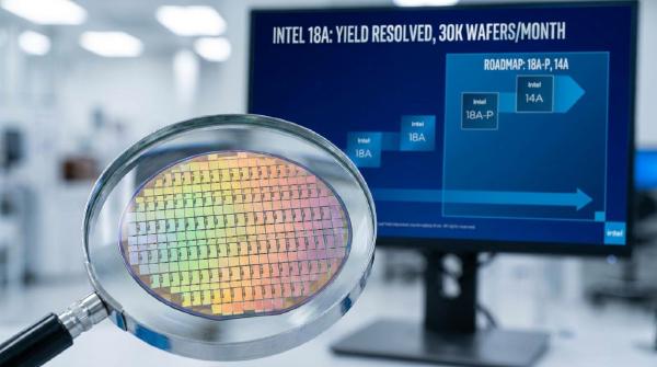
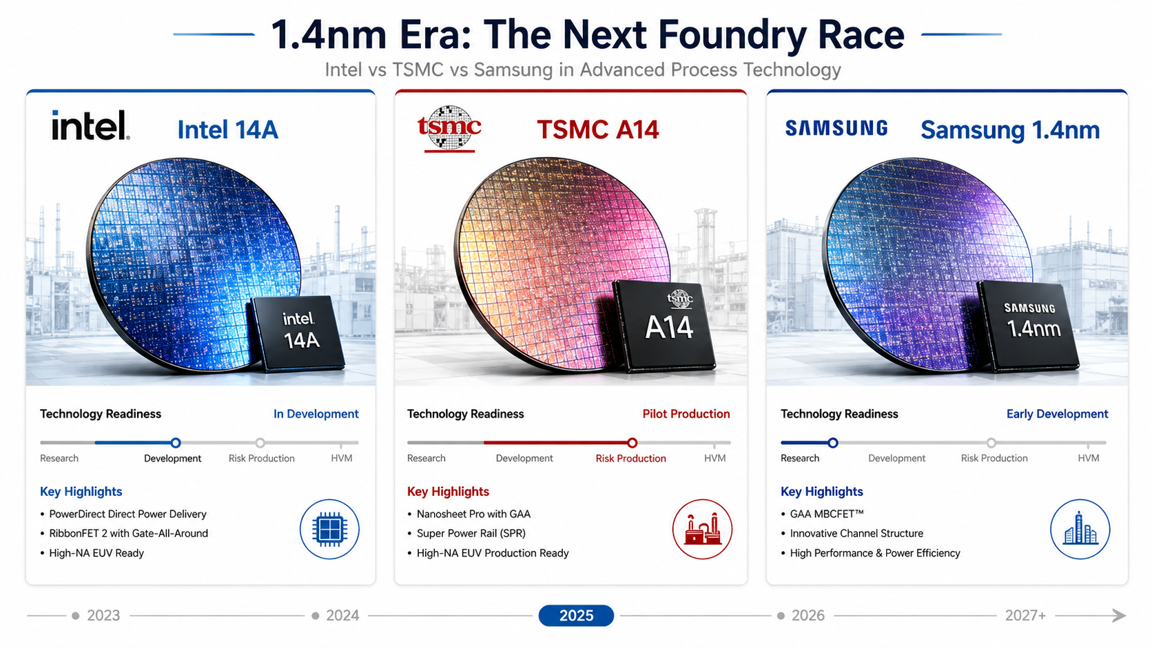
TSMC is expected to begin production of its A14 process in the coming years, while Samsung continues progressing toward commercializing its own 1.4nm-class technology. Against this backdrop, Intel has been preparing its 14A process as the successor to its 18A family, with several external customers already expressing interest in utilizing Intel Foundry services.
According to industry reports, Intel is now considering adding 14A Gen2 (14A2) to its roadmap.
Rather than replacing the base 14A technology, 14A2 is expected to serve as a refined second-generation implementation that improves manufacturing efficiency, transistor scaling, and power delivery while strengthening Intel’s competitive position in the advanced foundry market.
⚙️ Key Architectural Enhancements in 14A2 #
The proposed 14A2 node builds upon the technological foundation established by the standard 14A process.
PowerDirect and Backside Power Delivery #
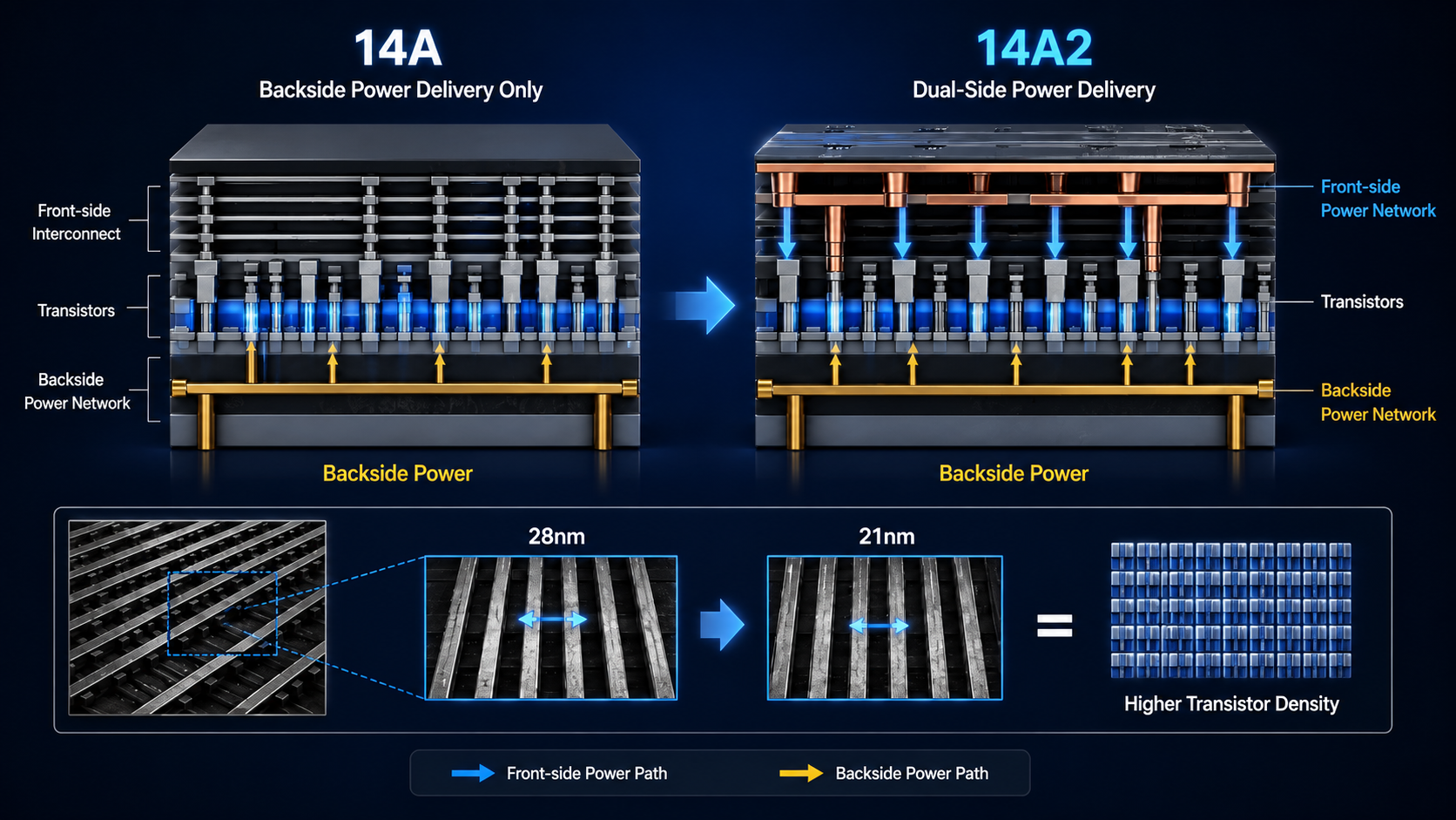
The baseline 14A node incorporates Intel’s PowerDirect technology, which utilizes a Backside Power Delivery Network (BSPDN).
Separating power routing from signal interconnects offers several advantages:
- Reduced routing congestion
- Improved power integrity
- Better transistor utilization
- Greater scaling opportunities for advanced designs
The original 14A process reportedly features:
- 28 nm M0 metal pitch
- Approximately 30% higher transistor density than its predecessor
- Full support for advanced High-NA EUV manufacturing
These capabilities already position Intel among the industry’s most aggressive process technology developers.
Dual-Sided Power Delivery #
The most significant enhancement planned for 14A2 is the introduction of a dual-sided power delivery architecture.
Instead of relying exclusively on backside power routing, the design distributes power through both:
- Front-side metal layers
- Backside power network
This hybrid architecture is intended to improve overall power distribution while supporting increasingly dense transistor layouts.
Smaller Interconnect Pitch #
Intel also plans to reduce the M0 metal pitch from:
- 28 nm → 21 nm
This substantial reduction enables:
- Higher routing density
- Increased transistor integration
- Better utilization of High-NA EUV lithography
- Improved manufacturing efficiency per exposure tool
Smaller pitches allow more circuitry within the same silicon area, improving both performance-per-area and manufacturing economics.
🔬 Engineering Challenges Behind 21 nm Scaling #
As with every new semiconductor generation, shrinking critical dimensions introduces significant engineering challenges.
Reducing the M0 pitch to 21 nm increases electrical resistance throughout the power delivery network.
Existing nano Through-Silicon Via (nTSV) structures reportedly become less effective at supporting the increased current density required by such compact layouts.
Without architectural adjustments, this could negatively affect:
- Power stability
- Signal integrity
- Thermal characteristics
- Overall manufacturing yield
Addressing these issues is essential before large-scale production becomes practical.
🏗️ Hybrid Power Delivery Strategy #
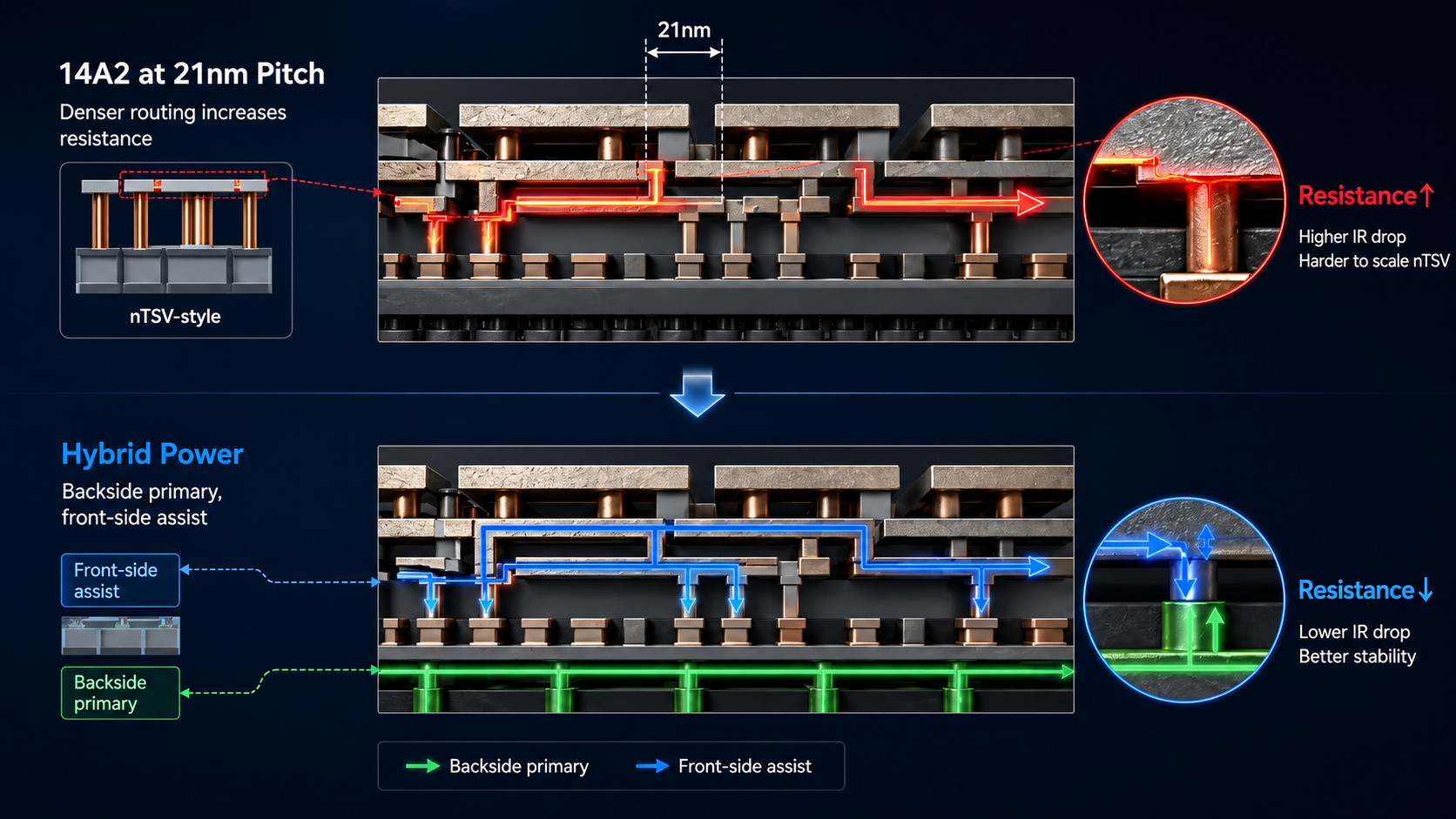
To overcome these limitations, Intel is reportedly developing a composite power delivery solution.
Instead of abandoning backside power delivery, the company intends to keep BSPDN as the primary source while shifting part of the electrical load onto conventional front-side metal layers.
This hybrid approach offers several potential advantages:
- Reduced electrical resistance
- Better current distribution
- Improved power stability
- Greater scalability for dense transistor arrays
If successfully implemented, dual-sided power delivery could become an important differentiator for Intel’s future process technologies.
🤖 Growing AI Demand Creates New Foundry Opportunities #
The timing of Intel’s roadmap expansion aligns with unprecedented demand across the semiconductor industry.
Artificial intelligence accelerators, cloud infrastructure, and high-performance computing continue driving record wafer demand.
Meanwhile, TSMC’s leading-edge manufacturing capacity remains heavily utilized by major customers, creating opportunities for alternative foundries capable of delivering competitive process technologies.
For many chip designers, additional manufacturing options reduce supply chain risk while improving access to advanced production capacity.
Intel aims to capitalize on this environment by positioning its foundry business as a viable alternative alongside TSMC and Samsung.
📈 Strategic Importance for Intel Foundry #
Intel’s foundry ambitions extend beyond developing cutting-edge process nodes.
Success ultimately depends on demonstrating:
- Competitive manufacturing yields
- Reliable production schedules
- Strong process maturity
- Cost-effective wafer production
- Long-term customer confidence
The company is steadily building a broader portfolio of advanced manufacturing technologies, including:
- 18A
- 18A-P
- 14A
- Proposed 14A2
Together, these nodes are intended to address diverse customer requirements across AI processors, data center chips, networking silicon, and next-generation consumer devices.
🏁 Outlook #
Intel’s reported 14A2 process represents more than a routine process refinement. By introducing dual-sided power delivery, tighter interconnect scaling, and enhanced utilization of High-NA EUV lithography, the company appears to be laying the groundwork for stronger competition in the 1.4nm-class manufacturing era.
Whether 14A2 ultimately reaches production according to plan will depend on Intel’s ability to solve the engineering challenges associated with increasingly aggressive scaling while maintaining high yields and manufacturing reliability.
As AI-driven semiconductor demand continues to accelerate, the success of Intel’s expanding process roadmap could play a significant role in reshaping the competitive balance among the world’s leading foundries.