Intel 18A-P Process: 1.8nm Performance Node and Diamond Rapids Xeon
🧠 Overview: Intel’s 1.8nm-Class Performance Node Enters Risk Production #
Intel Foundry has announced that its enhanced process variant, Intel 18A-P, has entered risk production, marking a key milestone in its 2nm-class manufacturing roadmap.
Introduced as a performance-optimized evolution of Intel 18A, the new node targets improved efficiency, thermal behavior, and design flexibility for next-generation high-performance computing (HPC) and AI workloads.
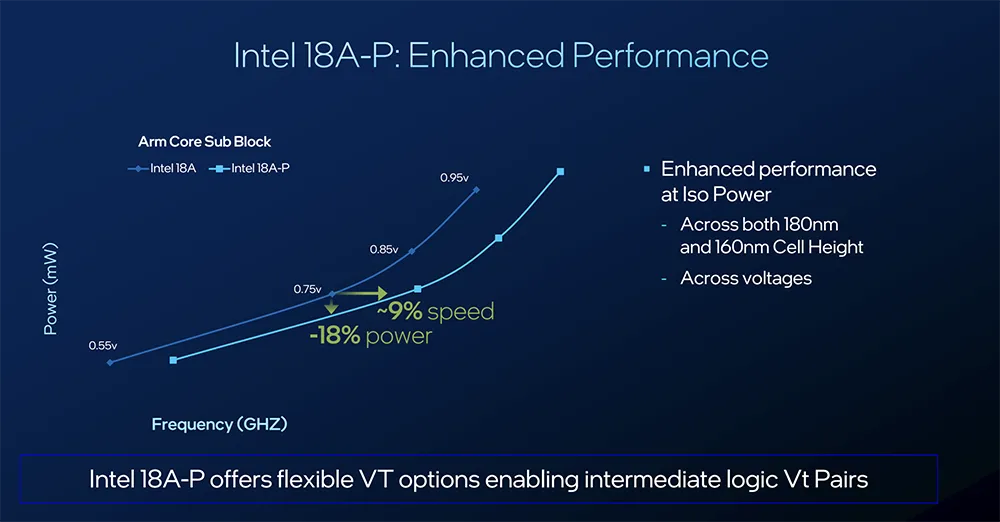
Benchmarks based on standard Arm core test modules indicate:
- +9% performance at iso-power, or
- ~18% power reduction at iso-performance
This positions 18A-P as a refinement node aimed at maximizing efficiency gains without altering core design rules.
⚙️ 18A-P Node Positioning: Evolution of Intel 18A #
Intel 18A-P is designed as a drop-in enhancement to the baseline 18A process, maintaining full design compatibility while improving electrical and thermal characteristics.
Key Positioning Attributes #
- Node Class: 2nm-class (Intel “18A” angstrom branding ≈ 1.8nm)
- Variant Type: Performance-enhanced derivative of 18A
- Compatibility: Full design-rule compatibility with 18A
- Target Markets: HPC, AI accelerators, and server CPUs
This compatibility ensures IP reuse and seamless migration for existing 18A designs.
🔧 Process Enhancements: Transistors, Power, and Variation Control #
Intel 18A-P introduces multiple physical and electrical improvements across transistor design, power delivery, and variability reduction.
Transistor-Level Improvements #
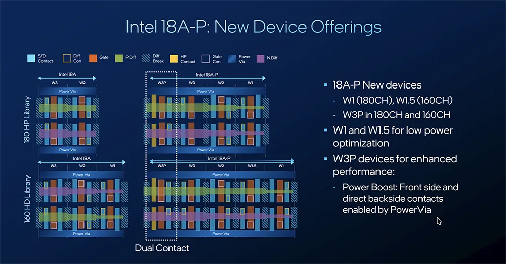
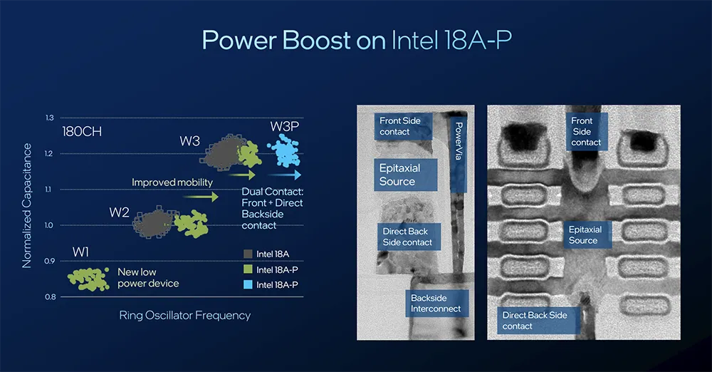
- Expanded transistor width options:
- Ultra-low power variants (W1, W1.5)
- High-performance dual-contact W3P design
- Improved drive current without proportional capacitance increase
- Enhanced switching efficiency for performance-sensitive workloads
Power Delivery Enhancements #
- Extended use of PowerVia backside power delivery
- Dual-contact architecture reduces resistance paths
- Improved voltage stability under load
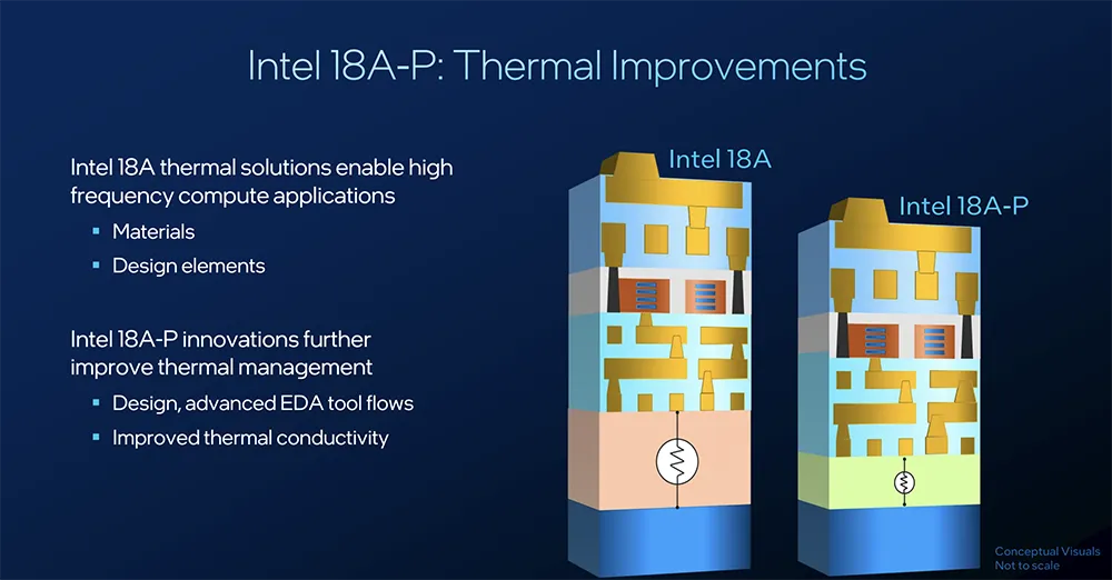
Thermal and Resistance Improvements #
- 20%–40% reduction in thermal resistance
- 10%–30% reduction in via resistance
- Improved heat flow paths via vertical interconnect optimization
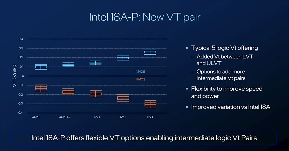
Variability and Voltage Optimization #
- Threshold voltage (Vt) expanded with additional fine-grained option
- 33% reduction in process variation spread
- Better guard-band utilization for higher sustained performance
🧠 RibbonFET and GAA Scaling #
Intel continues scaling its Gate-All-Around (GAA) transistor technology under the RibbonFET architecture.
RibbonFET Design #
- 4-nanoribbon transistor structure (vs. 3-nanosheet designs in competing implementations)
- Higher drive current density
- Improved switching efficiency at advanced nodes
GAA + PowerVia Synergy #
Combining RibbonFET with backside power delivery delivers:
- ~11% routing area reduction
- Up to 10× reduction in IR drop
- ~6% frequency uplift or >15% power savings
- ~30% frequency gain at ultra-low voltage (~0.5V scenarios)
This combination is central to Intel’s scaling strategy beyond FinFET.
🚀 Diamond Rapids Xeon: First Major 18A-P Deployment #
Intel’s next-generation server CPU family, Diamond Rapids Xeon, will be one of the first major deployments of 18A-P technology.
Expected Specifications #
- Core Count: Up to 192 cores
- Tile Configuration: 4 compute tiles
- Architecture: P-core-based server design
- Process Node: Intel 18A-P
Each compute tile integrates:
- 48 high-performance P-cores
- Large shared L3 cache structures
- Advanced chiplet interconnect fabric
The architecture is optimized for AI workloads, HPC simulations, and large-scale cloud computing environments.
📊 Design Flexibility: Multi-Library Cell Strategy #
Intel 18A-P supports multiple library configurations to balance power and performance:
- 180nm cell library: optimized for low-power designs
- 160nm cell library: high-density performance configurations
This dual-library approach allows designers to tune silicon for:
- Energy efficiency (mobile/server efficiency cores)
- Peak performance (HPC and AI acceleration)
🧬 Advanced Research: Post-2nm Roadmap #
Intel also outlined long-term semiconductor research directions beyond 18A-P:
CFET Scaling #
- Vertical stacking of NMOS and PMOS devices
- Gate pitch reduced to ~45nm
- Pathway beyond GAA scaling limits
GaN + Silicon Integration #
- Monolithic integration of GaN power devices with silicon logic
- Enables high-efficiency power management on-chip
- Targets system-level simplification for advanced electronics
Ruthenium Interconnects #
- Replacement for copper at advanced scaling nodes
- ~35% capacitance reduction using subtractive ruthenium structures
- Improved frequency scaling headroom for future nodes
📉 Industry Context: The 2nm Competition Era #
With the industry entering the 2nm-class process generation, competition among leading foundries is intensifying.
Intel 18A-P positions the company to compete directly with:
- TSMC N2-class nodes
- Samsung SF2-class technologies
The emphasis is shifting from pure node shrinking to:
- Power efficiency per watt
- Thermal scalability
- AI workload optimization
- Interconnect density and performance stability
📌 Conclusion: A Refinement Node for AI-Driven Compute #
Intel 18A-P represents a strategic refinement of Intel’s 2nm-class process technology rather than a full architectural reset.
By improving performance-per-watt, reducing thermal resistance, and enhancing variability control, Intel is strengthening its manufacturing foundation for next-generation AI and HPC workloads.
With Diamond Rapids Xeon as a flagship deployment vehicle, 18A-P is positioned as a key enabler for large-scale data center evolution in the 2027 timeframe and beyond.